Andre Adrian, DL1ADR
version: 2026-06-26
The words microprocessor, microcomputer and microcontroller are
related, but describe different kinds of "micro". First, micro is
another word for Large Scale Integration (LSI) computing devices
that appeared in the 1970s. One early example is the "Calculator-on-a-Chip"
Mostek MK6010. This IC contained the CPU, ROM, RAM, IO in one
housing and is a mask-programmed
microcontroller by todays wording. The Zilog Z80 and MOS
Technology 6502 are examples of microprocessors, that is only the
CPU is in the IC, ROM, RAM, IO are external. There was always a
limit of maximum number of transistor functions on a IC. Therefore
"CPU only" microprocessors have more computing power then the
microcontrollers of the same vintage. A microcomputer is the final
product. Be it a game console like Atari 2600, a home computer
like Commodore C64 or a personal computer (PC) like IBM PC.
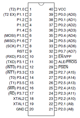
This web page describes a 8052 microcontroller computer. The Intel 8048 or MCS-48 was first released in 1976. The Magnavox Odyssey 2 game console from 1978 used the 8048 microcontroller instead of a microprocessor. The Intel 8051 or MCS-51 was the more powerful follow-on and first released in 1980. I use the Atmel AT89S52, a microcontroller with Flash memory as ROM. The classic 8048 was mask programmed. The 8748 has EPROM.
The 8052 microcontroller RAM has a small size of 256 bytes. The
8052 allows external program and read/write memory. An external 32
KByte SRAM allows program download thru the build-in UART (serial
port). An UART-to-USB bridge with CP2101 or FT232 completes the
connection to the host computer.
There is discussion about "the first microprocessor" and there is
discussion about "the first microcontroller". The Intel 8080 had
real impact on the market, think of S100 bus and CP/M operating
system, earlier microprocessors had not. The first
microcontrollers had little impact. The german company Olympia
produced the CP-3F, the
german company Nixdorf the NCF1.
Other microcontrollers are SGS-Ates
M380 and General Instruments LP8000. The most prominent of
this bunch was Fairchild F8.
There was a dispute between Olympia (AEG) and Fairchild about "who
stole from whom". Instead of a court battle, both
parties made a license agreement. The Fairchild F8 was, like
the CP-3F and the others, a two chip microcontroller. The second
chip contains the program counter (PC), ROM and IO. The first chip
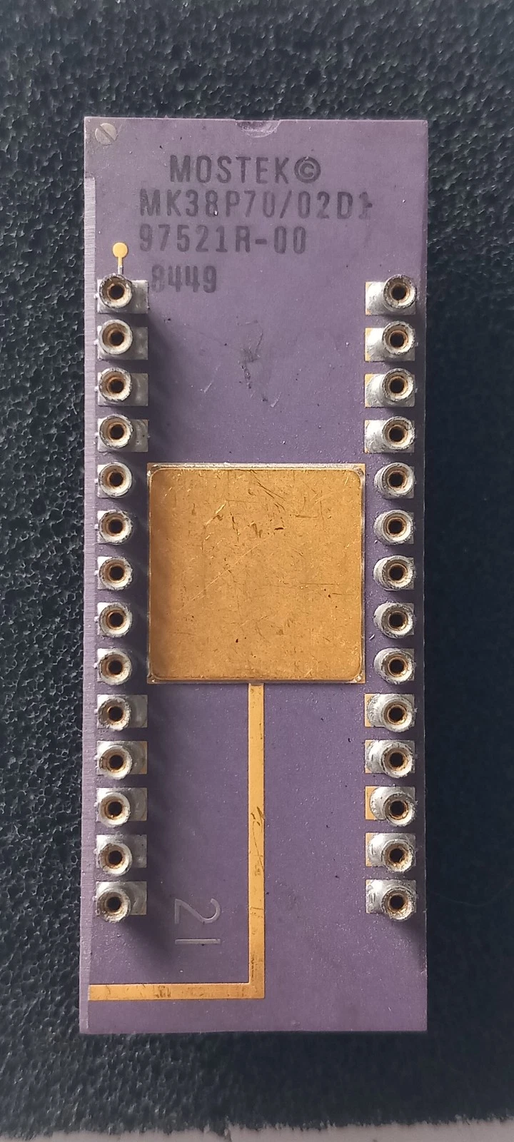
contains the CPU and "scratchpad" RAM. The Mostek MK3870 combined
both F8 chips into one. There was a mask-programmed version like
the MK3870/42 with 4KByte ROM and 64 Bytes RAM. The MK38P70 was
for development. A "real" EPROM is placed on top of the MK38P70:
The Mostek MK3870 can not use external ROM or RAM. The Intel
MCS-48 and MCS-51 range of microcontrollers can. There are
ROM-less versions like the 8040 (MCS-48) and the 8032 (MCS-51).
The Intel microcontrollers are called "Harvard
architecture", that is separate program and data memory. In
my opinion, there is no "real" Harvard architecture. You can
combine /PSEN and /RD CPU outputs to use external RAM for program
AND data memory.
The Fairchild F8 or Mostek MK3850 were used in one of the first
chess computers, the CompuChess
from 1977. This time, the firmware (ROM program) was stolen by Novag
Chess Champion MK1. See the case Data
Cash Systems v. JS&A. A friend of mine had the Novag MK1
chess computer. It played horrible chess ...
The CompuChess binary file is 32014-4950_cmcsi_staid.u3. The
hardware was 2 KByte ROM, 256 Byte RAM controlled by MK3853 and 64
Byte Scratchpad RAM. My idea to run CompuChess on 38P70 is not
working. The 64 Bytes scratchpad RAM shall be enough for a pocket
calculator program. Traditionally this is done in BCD arithmetic
to avoid binary to decimal conversion. The simulator MAME can
execute the CompuChess program with the CompuChess
MAME driver.
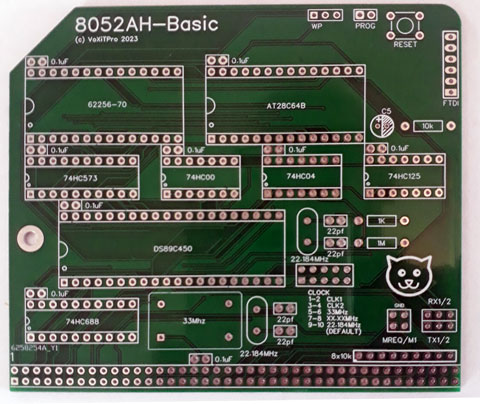
Ronald Dekker build a tiny
80(C)32 BASIC board. The 8032 is a ROM-less MCS-51 variant.
I use the AT89S52 with 8KByte ROM. I want to port the monZ80
monitor (BIOS) from the Z80
blinkenlights computer to MCS-51 microcontrollers. Then I
want to run MCS BASIC-52 from 1985. This late BASIC has
one-dimensional DIM, 6-bytes BCD floating point numbers and
IF-THEN-ELSE.
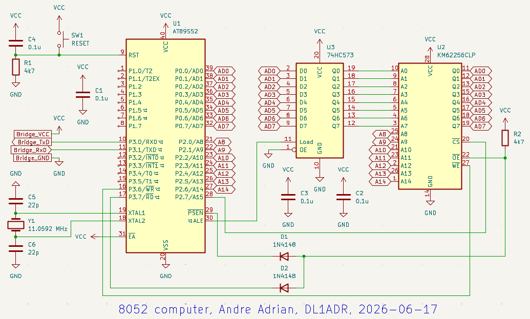
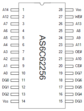
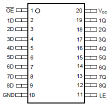
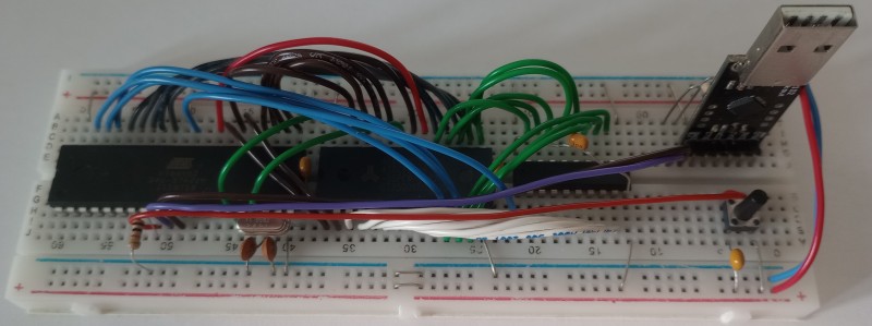
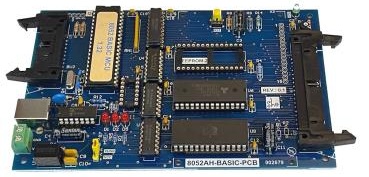
The number of integrated circuits or "chips" is small. The
CPU/ROM/IO AT89S52, the RAM AS6C62256, a low power 32 KByte SRAM,
and one glue chip 74HC573. A "diode logic" AND gate out of diodes
D1, D2 and resistor R2 combines the /PSEN and /RD output of the
CPU to create a "von
Neumann" computer architecture with combined program and
data memory. The octal latch 74HC573 de-multiplexes data-bus and
lower address-bus for the RAM. Last but not least a ready-made PCB
with UART-to-USB bridge is used.
The +5V voltage supply (VCC) for the 8052 computer runs thru the
UART-to-USB bridge. The capacitor C1 is placed next to U1, C2 next
to U2 and so on.
 |
 |
 |
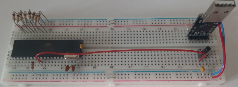
A "NOP tester" is a simple set-up to test the CPU. The
traditional schematic wires the NOP opcode to the databus,
connects a clock source and uses a Logic Analyzer to check
the CPU signals like memory-read, memory-write.
For the AT89S52 I use "External access", that is pin /EA=GND. The
databus is wired to opcode 74h, the "MOV A,#74h" opcode. The
quartz and the reset push button are wired as in the 4-chips 8052
computer above. The AT89S52 is placed left, the USB-to-UART bridge
and reset push button is placed right. In between is place for RAM
and 74HC573:
The "MOV A,#74h" has a length of 2 bytes, first for opcode,
second for immediate value. The duration is one cycle. A cycle is
12 oscillator clocks or two ALE cycles. The following "Program
memory read cycle timing" diagram is from the 8051
Architectural Specification and Functional Description. More
information is in MCS
51 Microcontroller Family User's Manual.
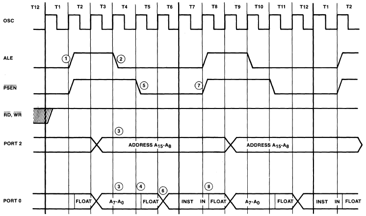
The first Logic Analyzer screenshot shows the details of MCS-51
code memory opcode fetch. The Address Latch Enable (ALE) signals
if the AD-bus carries address-bus (ALE=1) or data-bus (ALE=0)
information. In detail, the ALE falling edge, the transition from
1 to 0, signals valid address.
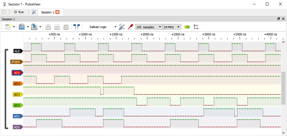
At the rising edge of /PSEN the value on the AD-bus is copied into
the CPU to the instruction decoder (first byte) or A register
(second byte).
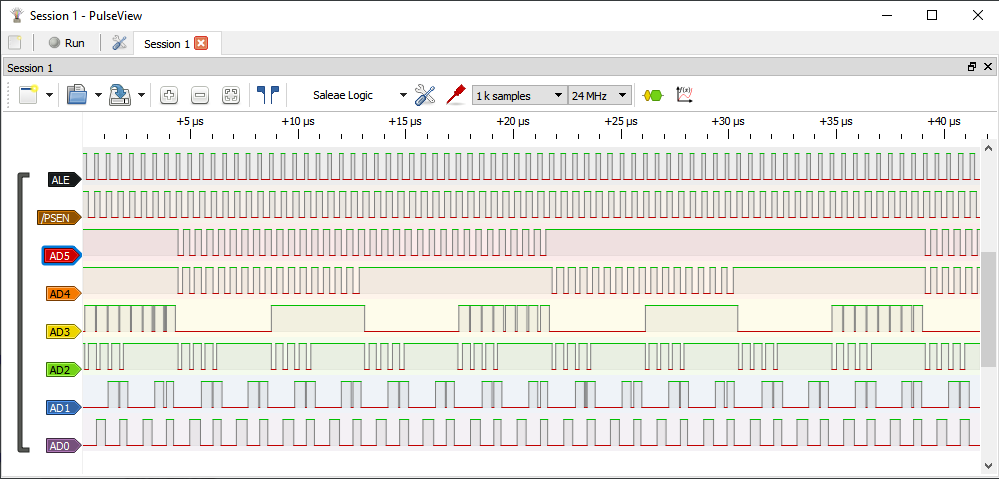
The second Logic Analyzer screenshot shows the "memory walk" with
a longer duration. The AD-bus lines AD0, AD1, AD3 are pulled low
(logic 0, GND). If the AD-bus is not emitting high (logic 1, VCC)
in the address output phase, the value is low. The AD-bus lines
AD2, AD4, AD5 are pulled high. If we consider the differences
between pull low and pull high, we can see that the CPU emits
increasing PC values.
Intel published 8052
BASIC versions 1.0 and 1.1 Operating and Reference manual.
Elektor magazine extended this BASIC by I2C
commands and in version
1.3 for more various types of controllers like Dallas
80C320. Anthony, F4GOH, offers 8052 BASIC version
1.31 on Github for his 8052 PCB. The file AT89S52@DIP40.HEX
is all you need to program. I use the Xgpro TL866II programmer.
The 8052 BASIC detects the baudrate (bps) automatic. I tested
successful 9600 bit/s and 19200 bit/s with the terminal emulator
program Tera Term. After pressing reset on the 8052 computer,
press SPACE key on the terminal emulator computer to get the
MCS-BASIC hello message:
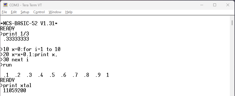
The baudrate automatic detect sets the "Special function operator"
XTAL, that you can see with a PRINT command. The 8052 BASIC has a
feature set between Tiny BASIC and full featured
(Microsoft-)BASIC. The 8052 BASIC uses 8 digit BCD floating point.
The Tera
Term Home Page has on june 2026 the version 5.6.1, the
binary version is on heise
download. This version has a working "Paste delay per line"
that is necessary for download BASIC listing to 8052AH BASIC.
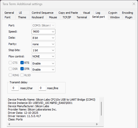
The first configuration is baud rate with menu "Setup|Serial
port..." and select 9600, 8n1 (8 data bits, no parity, 1 stop
bit):
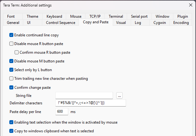
Now select tab "Copy and Paste" and set "Paste delay per line" to
600 milliseconds:
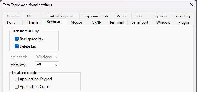
Third select tab "Keyboard" and activate "Transmit DEL by:
Backspace key". The line editor of 8052AH BASIC uses DEL character
(ASCII code 127 or 07Fh) as backspace character.
Last select menu "Setup|Save setup...". I use the default
TERATERM.INI. There are more options like black text on white
background or font "System" that I select.
The
Microcontroller Idea Book by Jan Axelson contains
information about 8052AH BASIC and input/output circuits. The hex2ram.bas program from appendix B
copies a hex file into 8052 memory. The first assembler program first.asm in chapter 13 is:
org 3000h ;location where
program will
;load in RAM
cpl p1.0 ;complement Port
1, bit 0
;(pin 1)
ret ;return to
BASIC-52
end
The hex file of first.asm is first.hex.
After downloading hex2ram.bas with CTRL-A, CTRL-C to copy the
BASIC program in the editor and ALT-V to paste the BASIC
program in Tera Term, you "run" the BASIC program and copy/paste
first.hex the same way. I exit the HEX2RAM program with some
invalid input.
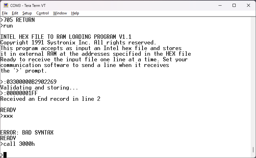
The assembler program is executed with "CALL 3000H". Every time
you execute the CALL, the output voltage on pin 1 of the AT89S52
changes from near 0V to near 5V or vice versa.
The "System Control Value" MTOP reserves data/program memory for
assembler programs. The following BASIC statement frees the range
from 6000H to 7FFFH for assembler programs:
IF MTOP=32766 THEN MTOP=MTOP-8192
Ultramon
is a MCS-51 monitor by Larry Cameron. The file ULTRAMON.HEX
uses all 8 KByte of the AT89S52 Flash ROM. The monitor is working
fine at 11.0592 MHz clock with 9600 bps, 8n1 (8 data-bits, no
parity, 1 stop-bit). After you pressed reset button, you have to
enter a key (SPACE) for automatic baud detection:
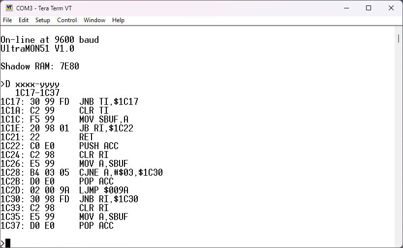
I use "Shadow RAM" at 0x7E80, the end of RAM in my 8052 computer.
The Ultramon has built-in single pass assembler, disassembler
and single step execution. The screen shot shows the
disassembly of subroutine OUTCHAR at 0x1C17. Two details I don't
like: there is no download to the 8052 computer in Intel hex
format. There is download and upload with XMODEM protocol. And
second, on Github is a working Hex file of Ultramon, but no source
code. Still, many thanks to Mustafa Kemal Peker for hosting.
After the powerful UltraMON51 without source code and the buggy
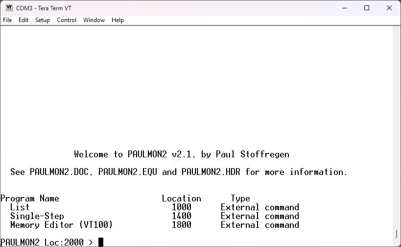
MON51, there is Paulmon2
by Paul Stoffregen. This monitor uses AS31 syntax that is not
compatible to C51ASM syntax. But you can download the hex file
pm2_2.obj. I renamed pm2_2.obj to pm2_2.hex to make the programmer
TL866II find it.
The Paulmon2 monitor needs the RETURN key to autodetect
the baud rate:
The book "The 8051 microcontroller" by Scott MacKenzie contains in appendix G the MON51 monitor (BIOS) program in 10 source files. This program can download Intel Hex files into 8052 RAM and execute it. Vahid Heidari has the MON51 assembler source code on Github. The original source needs the Intel ASM51 assembler and Intel RL51 linker.
I selected the free (as in free beer) Microchip (Atmel) C51ASM. This assembler needs all assembler source code in one file. You can use the "assembler control" $INCLUDE to cheat the one-file restriction and include 9 source files into the "one file". The original MON51 uses macros. The C51ASM has macros, too, but the syntax is different. At the moment I can assemble and execute my C51ASM version of MON51, but there are errors.My assembler toolchain does not use an IDE (Integrated Development Environment), but it is free (as in free beer). I use on MS-Windows:
Notepad++ as source code editor
CMD as MS-Windows shell (OS-prompt)
C51ASM as assembler
XVI32 as binary editor to "trim" the Bin file
TeraTerm as terminal emulator/XMODEM transfer program
UltraMON51 on 8052 computer as monitor
First some preparations. To start CMD.exe, press Windows key and
R to start the "Run popup" and enter "cmd". Second, to add the
directory of C51ASM executeable (C:\mybin) to the PATH variable,
enter:
path=%path%;C:\mybin
A simple test program is iotest.asm :
cseg
org 2000h
lcall OUTSTRING
db "Hello
8051", 0
lcall INCHAR
ljmp RESET
end
The C51ASM uses CSEG to select the code segment. The PROGRAM RAM
at my 8052 computer starts at 0x2000. The complete ASM file has
definitions for OUTSTRING, INCHAR and RESET. The source file is
assembled with
c51asm iotest.asm -fB -l
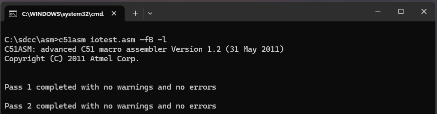
This command creates a binary file iotest.bin
and a list file iotest.lst. The binary
file starts at address 0x0000, therefore it is larger then 8
KBytes. The XMODEM program in TeraTerm needs only the part
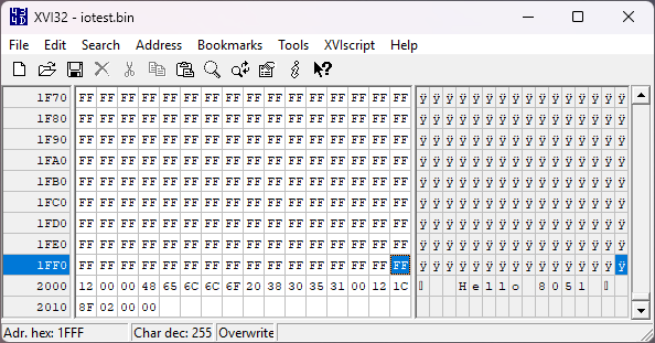
starting at 0x2000. I use XVI32 to trim the binary file.
Load the iotest.bin file into XVI32, then place the cursor at
address 0x1FFF. Next select menu "Edit|Delete to Cursor" and save
the truncated binary file as iotest.bin.
Download the truncated binary with TeraTerm. First start the
download at the 8052 computer with the UltraMON51 "R 2000,04"
command, then start the download at TeraTerm with menu
"File|Transfer|XMODEM|Send..."
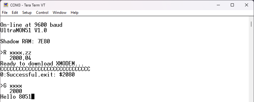
Last, start the program with "G 2000" at the 8052 computer.
Congrats, you executed another "Hello" program! Go back to
UltraMON51 with two times SPACE key.
A Google search for "8051 games" showed Snake
as top hit. The implementation uses a LED matrix of 8 times 8
LEDs. My version uses the keyboard of the Terminal emulator as
input and the ASCII display with ANSI escape sequences as output.
As starting point I use the repository MCU8051Games
by Danylo Polishchuk. First step on the way of "ANSI escape
sequences Snake" is to assemble the given source code. Some
modifications are needed for C51ASM. The first iteration is snake0.asm.
There are several C compilers for MCS-51. There is the Keil
PK51 commercial C compiler that has a demo version. Next is
the IAR
Embedded Workbench for 8051 which has a demo version, too.
The SDCC small device C
compiler is the GPL license alternative. I use SDCC version
4.5 for 64-bit MS-Windows. There are SDCC files
for 64bit MS-Windows, Linux and MacOSX.
I found a nice serialtest
C program on the internet. The program reads from MCS-51
UART, converts the character to upper case and sends this
character back to UART. Receive and transmit is without interrupt.
Some changes on the source code were necessary for SDCC 4.5
version and for 9600 baud (bps) operation at 11.0592 MHz CPU
clock:
#include <mcs51/at89x52.h>
#include <stdio.h>
#include <ctype.h>
int getchar (void) {
char c;
while (!RI); /* wait to
receive */
c = SBUF;
/* receive from serial */
RI = 0;
return c;
}
int putchar (int c) {
while (!TI); /* wait end of
last transmission */
TI = 0;
SBUF = c;
/* transmit to serial */
return c;
}
void UART_Init(void) {
SCON = 0x50; /* uart in mode 1 (8 bit), REN=1
*/
TMOD = 0x20; /* Timer 1 in mode 2 */
TH1 = 253; /* 9600 Bds at
11.0592MHz */
TL1 = 253; /* 9600 Bds at
11.0592MHz */
ES = 0; /* Disable
serial interrupt*/
EA = 0; /* Disable
global interrupt */
TR1 = 1; /* Timer 1
run */
TI = 1; /* enable
transmitting */
RI = 0; /* waiting to
receive */
}
void main(void) {
UART_Init();
for(;;) {
char c;
c = getchar();
c = toupper(c);
putchar(c);
}
}
The C file is serialtest.c. The file
for the AT89S52 programmer is serialtest.hex.
Some documentation to TH1, TL1 is confusing. The CPU clock is
divided by 12*32 that is 11059200/(12*32)=28800. The maximum baud
rate is 28800. Next step is to calculate the divider for the
wanted baud rate of 9600. 28800/9600=3. Last step is to calculate
256-divider=256-3=253.
The Atmel
8051 microcontrollers hardware manual explains the special
function register (SFR) like SCON, TMOD. The Atmel document UART
program examples explains UART operation in C and assembler
with interrupts.
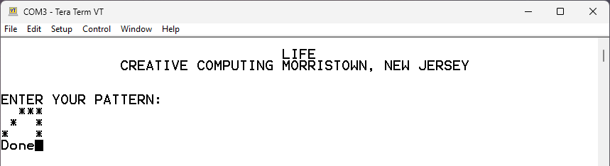
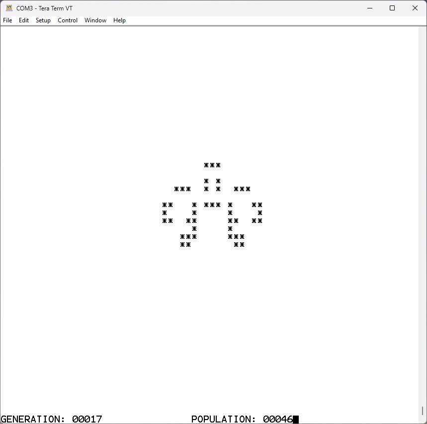
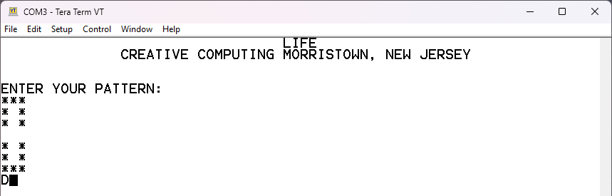
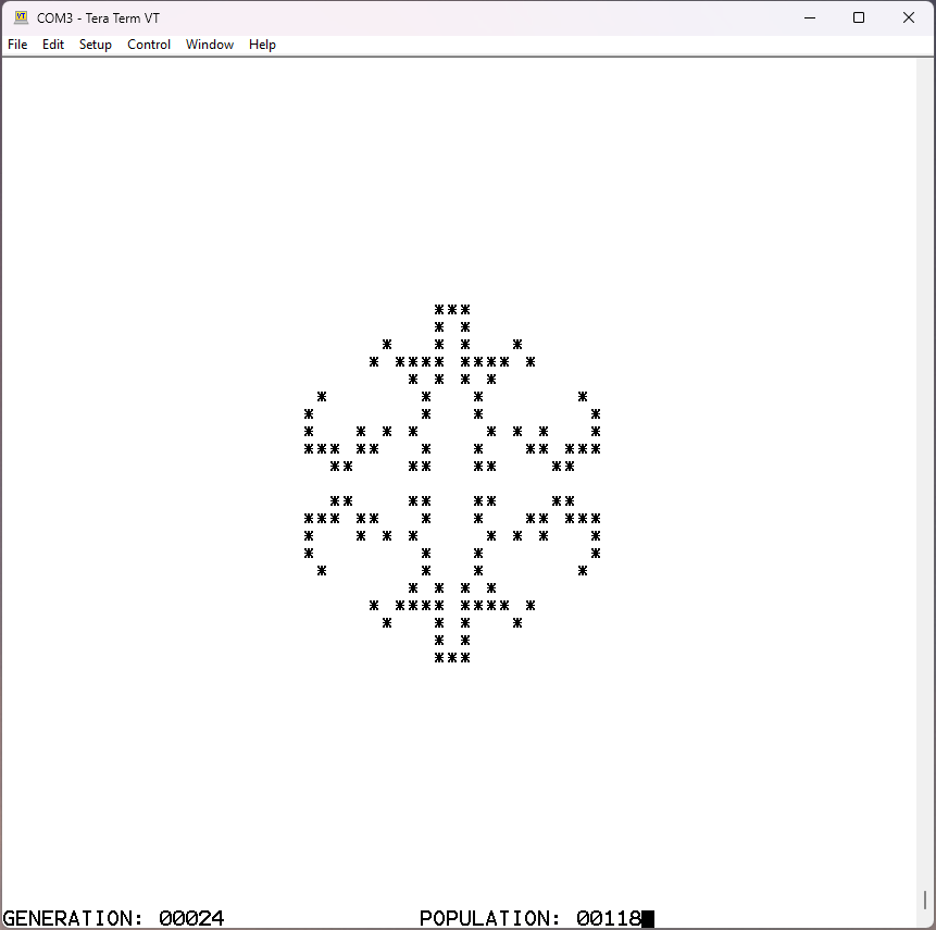
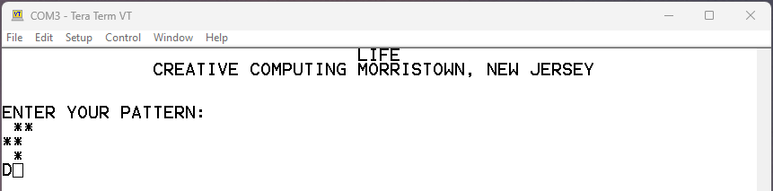
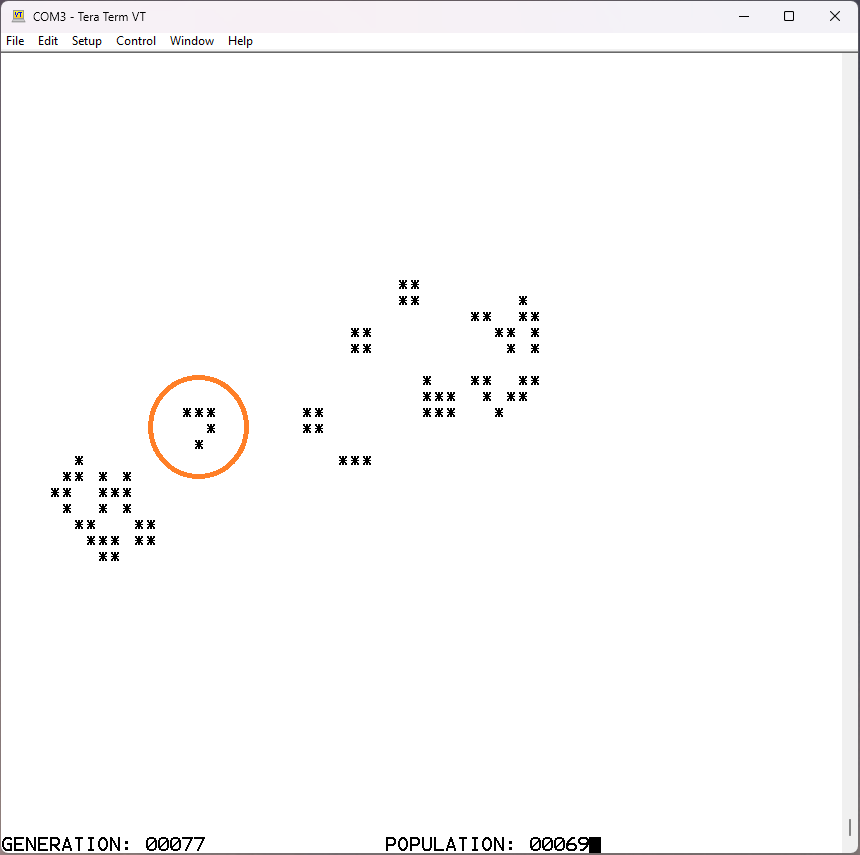
On my Z80 blinkenlights page I ported a BASIC
version of Game of Life to C. I took the Z80 HI-TECH C
compiler version and adapted it to the 8051 SDCC C compiler. There
were some name collisions with single letter names in the
at89x52.h file. The important difference was that the arrays AA
and BB have to be __far, that is, are placed in the external RAM.
Another difference is in the implementation of putcm() and
getcm().