Z80 blinkenlights
Author: Andre Adrian, DL1ADR
Version: 08.May.2026
Introduction
There are some internet pages about Z80 homebrew computers. The
Zilog Z80 and the Intel 8080 are both well known by me. My first own
microcomputer was a Sinclair ZX81 kit. Before I bought the ZX81 kit,
I tried to solder a 8080 system together. But I did not have the
knowledge nor the patience to succeed. That 8080 system of mine used
an 1KByte 2708 EPROM for a little monitor program I found in a
computer book. Before I could build my 8080 system I had to build an
EPROM programmer. The most simple solution I found was to connect
twenty switches to the EPROM data bus and address bus and a push
button switch for the programming voltage. EPROM programming was to
flip the switches and hit the "program" push button. The monitor
program was only 768 bytes long, but I soon gave up. There was too
much human error. At this time I had no EPROM eraser and I did not
know that to erase a EPROM it is sufficient to expose it to direct
sunshine for some hours. Over the years my more then primitive EPROM
programmer and the other parts of the 8080 project got lost.
Today we live in the age of laptop and USB. As another "nostalgia
project" I want to build the Z80 blinkenlights computer. For
the moment the Z80 blinkenlights specification requests only 64KByte
of static RAM, a RS232 port and a tiny monitor program of say
256Bytes. I do not want to spend much time on this project,
therefore there is no fancy stuff like a PS/2 adapter for a PS/2
keyboard or a graphics adapter for a VGA monitor or a Compact Flash
card as hard disk replacement.
The Z80 blinkenlights computer has to find its monitor program.
Again I have to build a programmer. This time it is a SRAM
programmer. Instead of switches and a program push button I
use an ATmega 16A microcontroller. This custom made "DMA
controller" connects the Z80 blinkenlights to my laptop through an
USB-UART bridge like Silicon Labs CP2102, CP2104 or FTDI FT232RL.
After building a 65C02 computer,
a 2650 computer
and a 6309
computer, I changed the schematics of the Z80 Blinkenlights to
28C64 ROM, 65C51 ACIA as in the 65C02 and 6309 computer. The CP2102
only "SRAM programmer" did not work stable,
reproducible.
Table of contents
Z80 blinkenlights
List of parts
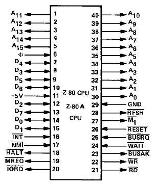
The most important part is the Z80. I have a Z84C0006. This is
the CMOS version for up to 6.17MHz clock speed. Within the Z80
blinkenlights the Z80 operate at 6.144MHz. One gate of a 74HC04
chip implements a Pierce quartz oscillator. Next to the quartz and
the 74HC04 two resistors and two capacitors are needed. The memory
of the Z80 blinkenlights is 64KByte static RAM. A CP2102, CP2104
or FT232RL USB-UART bridge on a tiny PCB connects the RS232
interface on TTL level to the "mainframe" computer, my
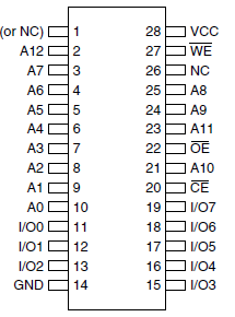
laptop. ROM is 8 KByte EEPROM 28C64 that contain monz80 monitor
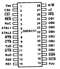
and Microsoft 8 KByte BASIC. RS232 interface is ACIA 65C51P2.
Clock generator
The Z80 needs a "single-phase MOS-level clock". The standard clock
generator circuit is the Pierce oscillator. As in every oscillator
there is a frequency dependent network and an amplifier. The
amplifier should be linear, that is the output signal should be a
scaled (enlarged) version of the input signal. There are no "real"
digital devices, just analog devices that are "tuned" in a specific
way. An inverter like the HCMOS 74HC04 has a high voltage
amplification and a low output impedance. There is a small input
voltage range where the output voltage depends on the input voltage.
In the Pierce oscillator circuit below the resistor R2 connects
inverter output to inverter input to give the input a bias to bring
the inverter into the linear region. The resistor R1 reduces the RF
power for the quartz. The quartz can only handle a tiny power.
Further R1 isolates the "analog" frequency dependent network from
the "digital" clock generator output. The quartz Q1 and the two
capacitors C1, C2 form a two port network. The input voltage is
applied at the two pins of C1, the output voltage is available at
the two pins of C2. The dependency from output voltage to input
voltage is linear, but frequency dependent. The quartz behaves for
the resonance frequency as a resistor of some 10Ω. Above and below
the resonance frequency the quartz has a high impedance. If we
switch on the oscillator there is only some thermal noise in the
circuit. Noise is a signal that contains all frequencies. Of all
these frequencies the resonance frequency of the quartz gets the
highest amplification. Sooner or later the supply voltage limits the
amplifier output voltage. The clock generator now produces a square
wave signal. Because the amplifier is not very linear, the duty
cycle is not exactly 50%, but a duty cycle of 45% to 55% is typical.
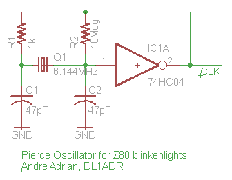
The following oscilloscope picture shows the output voltage of the
74HC04 clock generator. The load is one HCMOS input gate and the
capacitance load of a 10:1 oscilloscope probe. The oscilloscope
bandwidth is 200MHz. We see damped oscillations every time the
output voltage changes from nearly zero volt to nearly five volt or
back. This "over shoot" is due to inductances and capacitances we
can not avoid. Please remember, a piece of wire is an inductance and
every wire has a capacitive coupling to "earth" or "ground". The
inductance may be only some nano Henry and the capacitance may be
some pico Farad, but at a frequency of 6.144MHz they make an effect.
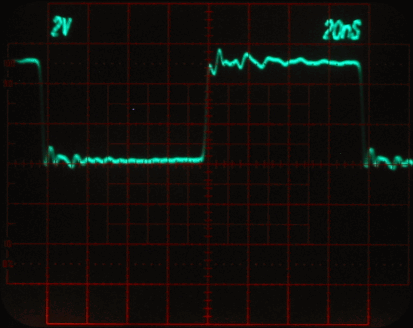
For the next oscilloscope picture a 4069 device replaces the 74HC04.
The 40xx logic family is older than the 74HCxx family. The 40xx
devices are slower and have a higher output impedance than the
74HCxx devices. The output of the 4069 clock generator is a
distorted sine wave. This picture should show everybody that there
is only analog electronics and digital electronics is just a
simplification. The 4069 has no "amplifier reserve". If we connect a
higher frequency quartz there will be no more oscillation.
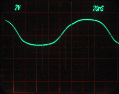
The last oscilloscope picture uses a 74AC04 as amplifier. The 74ACxx
logic family is faster than the 74HCxx family. We can see that
faster is not always better. The inverter oscillates at the delay
time frequency of the inverter, not at the resonance frequency of
the quartz. There are five oscillations per grid box in x direction.
One grid box has the "length" of 20 nano seconds. One oscillation
has a length of 4 nano seconds. As f = 1/T, the frequency is 1/4ns
or 250MHz. An analog oscilloscope can display information that is
above the oscilloscope bandwidth, a digital oscilloscope can not. We
have to assume that the voltage swing is larger than the display we
see, this is due to the low pass nature of the oscilloscope
amplifier. The resistor R2 connects amplifier output to amplifier
input- Parallel to this resistor there is a small capacitance of
some Pico Farad. Mostly it is the parasitic capacitance of the
breadboard connectors. The path through the parasitic capacitance
has a lower impedance than the path through the quartz. The circuit
behaves like a ring oscillator where the output of the inverter is
directly connected to the input and the signal travel time of the
inverter defines the output frequency.
Everybody can see that the 74HC04 device is the correct device for a
6.144MHz clock generator. In our case decision is easy. Sometimes
the tolerances of devices are large. Most examples of the device
behave as expected, but some examples behave like a sine wave
oscillator or like a ring oscillator. Because tolerances have a
Gaussian distribution, it is possible that we do not see the "worst
cases" at the lab bench, but only later in mass production.
The first Z80
blinkenlights experiment
What can we do with a clock generator and a Z80? We can build our
first blinkenlights experiment. The most simple CPU command or
opcode is NOP, no operation. The CPU reads the NOP opcode, does
nothing and increases the program counter. The next opcode is
fetched from the next memory location. If the next opcode is again
NOP, the program counter works like a binary counter.
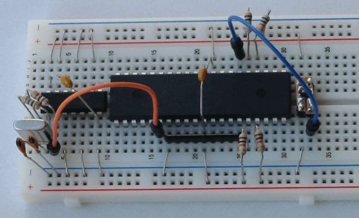
Picture: Z80 blinkenlights NOP test circuit. From left to right is
6.144MHz quartz, 74HC04, Z80 and MAX811 voltage monitor chip on an
adapter board.
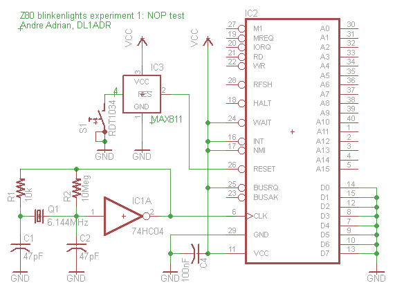
Picture: Z80 blinkenlights NOP test circuit schematics.
Hardware fun or
the meaning of data-sheet values
The supply voltage for the CMOS version for the Z80 is 4.5V to 5.5V,
according to the Z80 data sheet. What happens below 4.5V?
Microcontrollers of today have a supply voltage monitor function or
"brown-out detection" and stop program execution below the brown-out
voltage. My Z80 CPU performs the NOP test at a supply voltage of
1.2V, the lowest voltage my power supply can provide. I do not know
if the Z80 can execute every opcode at this low supply voltage
within the full temperature range. I only know that there are
chances that the Z80 will corrupt the battery buffered SRAM after I
switch of the power supply and the voltage drops slowly to zero
volts.
In the 1980s I worked with CMOS Z80 and battery buffered SRAM at my
job. It was quite a challenge to give the Z80 decent brown-out
capabilities. Finally we used a MAX690 chip. This 8 pin voltage
monitor chip did cost more than the Z80 CPU!
Logic Analyzer
measurements
I have a little 8-channel logic analyzer for the USB port. I like
to see the control bus signals to get a better understanding of
the datasheet timing diagrams and to check my glue logic circuits.
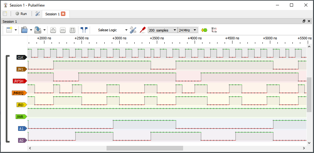
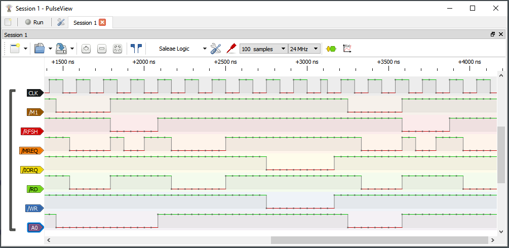
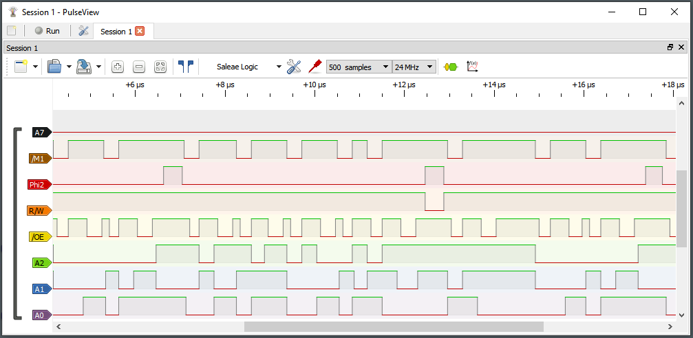
The first screen shot shows the Z80 executing the NOP opcode (0):
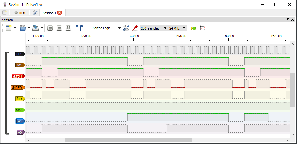
The datasheet says: NOP opcode has 4 clock cycles (4 T state). If
you look carefully, you see every 13 clock cycles one /M1 cycle.
And you see three /MREQ=low phases within these 13 cycles. The
first and third /MREQ=low is opcode fetch for two NOP opcodes, the
second /MREQ=low is a DRAM refresh. Summary: the measured Z80 does
not behave like the datasheet Z80.
NOP is not a typical opcode. A good NOP tester opcode is to load
an immediate value into a register, like the LD BC,0101h opcode
that is a 3 bytes opcode with coding 01h, 01h, 01h.
The datasheet says: LD BC,immediate opcode has 10 clock cycles (T
states). We can see this with the Logic analyzer. There are three
times /RD=low but four times /MREQ=low, because there is one
/RFSH=low DRAM refresh per opcode. We see that the memory access
time for a /M1 access is shorter then for a non-/M1 access. I
assume, the 150ns ROM 28C64 can handle Z80 8 MHz clock.
The Z80 OUT opcode is used to write to IO devices like the 65C51
ACIA. The opcode is 0D3h and is 2 bytes. If we wire 0D3h to the
data-bus, the opcode OUT (0D3h) is executed.
The datasheet tells the opcode has 11 clock cycles (T states) and
the Logic analyzer confirms this. There are two /RD accesses to read
the two bytes of opcode and there is one /WR access to write to the
IO device. The /IORQ access is longer then a memory access. The
65C51P2 needs at least 240ns for the Phi2=high phase. Again this is
fine for an 8 MHz Z80.
Z80 computer
There is a nice Z80 computer
schematics from Grant Searle. My schematics is a variant. I
use the 65C51P2 ACIA (2 MHz version) instead of 68B50 ACIA.
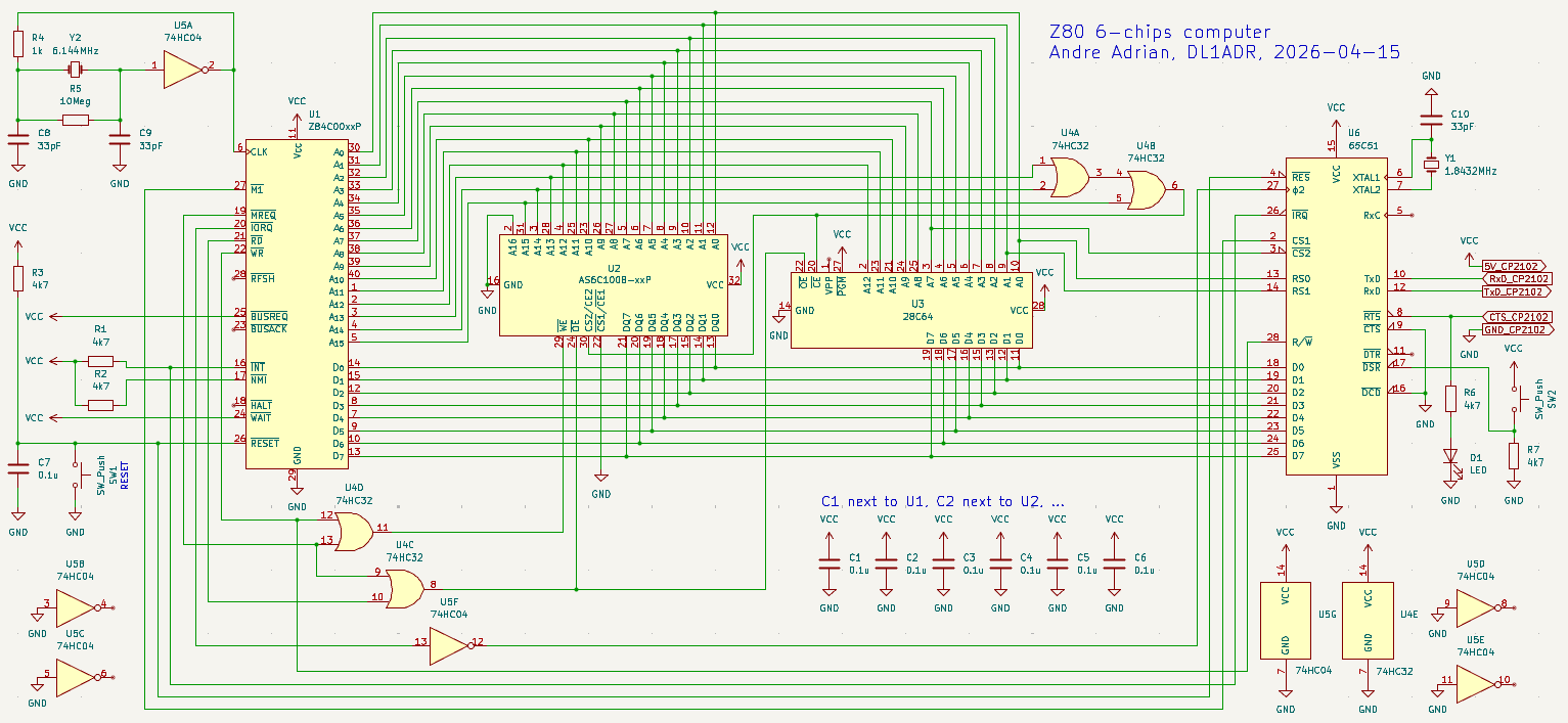
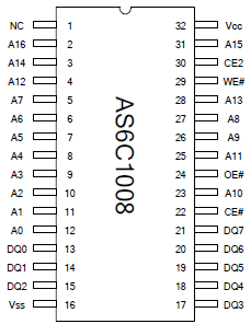
The ICs pinout 65C51, Z80, 6C1008 and 28C64:
The inverter U5A, the 6.144MHz quartz and the two 33pF capacitors
make a Pierce oscillator. The 10 Mega Ohm resistor R5 and C8 are
necessary for oscillation.
The lower 8 KByte are used for ROM, read-only memory. The upper 56
KByte are RAM, read-write memory. The ACIA uses IO address 7Ch to
7Fh.
The 28C64 ROM has access time of 150ns. This allows 8 MHz clock for
the Z80 CPU. The glue logic for /CE, /OE and /WE signals for ROM and
RAM is simple. The /CE for ROM and CE2 for RAM is logic OR of A13,
A14 and A15, created by U4A and U4B. The OR gate U4D creates /WE out
of /MREQ and /WR. U4C creates /OE out of /MREQ and /RD.
The control bus signals for 65C51 are CS1 (pin 2), /CS2 (pin 3),
Phi2 (pin 27) and R/W (pin 28). A7 is wired to /CS2. The CPU /M1
signal is used as ACIA CS1 to avoid confusion between IO read/write
access (/M1=high) and interrupt acknowledge (/M1=low). Inverter U5F
creates ACIA Phi2 signal out of CPU /IORQ signal. CPU signal /WR is
used as ACIA R/W.
The ACIA input /DSR is connected to push button SW2. The ACIA output
/RTS is connected to LED D1. See "first program" for more
information.
The Grant
Searle 6502 computer uses a neat trick to create RTS/CTS
hardware handshake: After a character is received by the ACIA, the
ACIA /IRQ output goes low. The inverted signal via U5E is used as
/CTS for the USB-UART (CP2102) bridge. After the CPU reads the ACIA
status register, ACIA /IRQ goes high and /CTS for USB-UART bridge
goes low.
Let's look at the /CEROM signal with the Logic Analyzer. This signal
is low, if A13, A14, A15 are low:
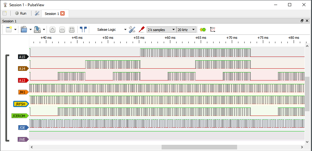
The Logic Analyzer display is a little confusing. For the lowest 8
KBytes of memory everything is as expected, but not for the other
memory addresses. A detailed Logic Analyzer screenshot shows why:
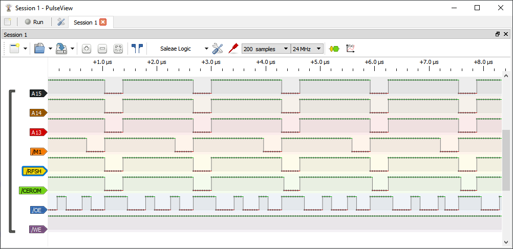
The DRAM refresh address counter runs free and creates /CEROM
signals while the CPU addresses memory above 2000h, the lowest 8
KByte. The "DRAM refresh noise" does not impact ROM or RAM, because
for activation of ROM and RAM there must be an active CE and either
/OE=low or /WE=low.
My Logic Analyzer is a toy, but good enough to show details of the
slow speed CPUs of the 1970s.
The first program
The first program uses the DSR input of the ACIA and the RTS output
of the ACIA. The level of the DSR input is copied to the RTS output.
If push button SW2 is open (not pressed), the LED D1 is dark, If SW2
is pressed, D1 lights. I use a "high brightness" white LED that
needs very low current. The following text is part of FIRST.LST, the assembler list file. The
assembler source is first.asm and the
binary file for the 28C64 ROM programmer is FIRST.BIN.
0000
forever:
; for(;;) {
0000 06
03
ld b,3
; B = RTS_High
0002 DB
7D
in a,(AC_ST) ; A = ACIA_status
0004 E6
40
and 40h
; A &= DSR_mask
0006 20
02
jr nz,endif ; if (A != 0) {
0008 06
0B
ld b,0Bh
; B = RTS_Low
000A
endif:
; }
000A
78
ld a,b
; A = B
000B D3
7E
out (AC_CMD),a ; ACIA_command = A
000D 18
F1
jr forever ; }
The first column is the address for the opcodes in the columns 2 to
5. The /M1 signal is low on fetch of the first byte of an opcode.
The program is discussed with the Logic analyzer scribe:
The ACIA is read with an IN opcode at address 07Dh. The ACIA read
happens at Phi2=hi and R/W=hi. The ACIA is written with an OUT
opcode at address 07Eh. The ACIA write happens at Phi2=hi and
R/W=lo.
Z80 blinkenlights
monitor (BIOS)
The monitor or BIOS program executes after a CPU reset. The monitor
program initializes the hardware, like configure the ACIA to the
correct speed. Then the monitor program enters the monitor command
loop. Traditionally the monitor has some primitive commands to read
and write the memory. The Z80 blinkenlights monitor is a port of my
6309
monitor.
The monitor prompt is \ (backslash).
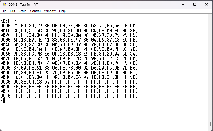
To print memory area FF00 to FFFE enter:
FF00:FFFEP
To enter values into memory, starting at address 0x3000, enter:
3000:11,2,AF,
The values are 0x11, 0x02, 0xAF. After EVERY byte a , (comma) is
needed.
To start a program at address 0x00BC enter:
00BCR
Lower case characters are converted to upper case. There is no input
line and therefore no line editing.
About the monitor language: minimum state and postfix. States are
necessary if something from the past is needed to handle the
present. For example, in LET B=A+1 the expression A+1 is part of an
assign, in IF B>A+1 the same expression is part of a compare.
Postfix is NOUN VERB, that is first the object, then the action. The
NOUN in the monitor language is a hexadecimal number of 1 to 4
digits, like 0, 19, AFFE or BA9. The VERBS are:
: to store the NOUN as 16-bit address in argA
, to store the NOUN as 8-bit value at address argA and increment
address argA
P to print the contents of the address range from argA to NOUN
R to run the program at address NOUN
CR (carriage return) to print CR, LF and the prompt
The BIOS has the following "operating system" subroutines:
0000h reset, start monz80
0008h putc, print output character in register A as ASCII
0010h getc, return input character in register A
0018h keybd, return input character available if register A
!= 0
0020h putcrlf, print carriage return, line feed
0028h putbyte, print output character in register A as
hexadecimal
The BIOS subroutines can be called by 3-byte opcode call 0008h,
call 0010h, ... or by 1-byte opcode rst 08h, rst 10h, ...
The assembler source file is monz80.asm.
The binary file for the programmer is MONZ80.BIN.
I used the MS-DOS program tasm as assembler. The Z80 monitor does
need some RAM space for stack. The two 16-bit monitor variables
accu (NOUN) and argA are registers HL and DE.
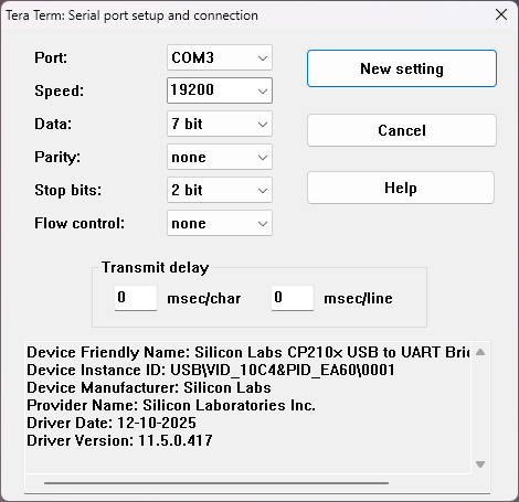
This Tera Term terminal emulator screenshot show the monz80 display
its binary code. The Tera Term setting is 19200 baud, 7N2 (7 data
bits, no parity, 2 stop bits) and RTS/CTS hardware handshake:
Microsoft (NASCOM)
BASIC
Grant Searle adapted Microsoft
BASIC to his Z80 computer. I made my Z80 monitor for ACIA
65C51 compatible to Searle's monitor for ACIA 68B50. Therefore the
BASIC assembler source needs no changes. I combined the monitor and
BASIC assembler source into one file monbas.asm
for easy ROM programming. The binary file is MONBAS.BIN.
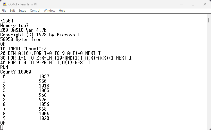
The BASIC cold start from monitor is 150R, the warm start is
153R. This is Microsoft 6-digit BASIC with 32-bit floating
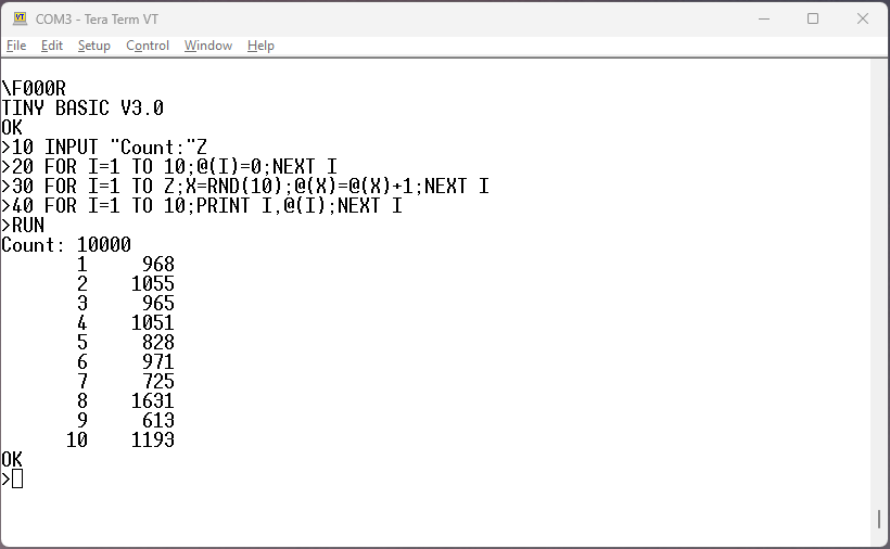
point numbers. The BASIC program rndtst2.bas
shows the quality of the RND() function.
There is a good NASCOM BASIC documentation (disassembly) in 80-BUS
News May-June
1983, July-August
1983, September-October
1983, November-December
1983, January-February
1984, March-April
1984 and May-June
1984.
The "NASCOM
8K BASIC Programmierhandbuch (german)" has the little BASIC
program hex.bas to convert hexadecimal number
to decimal number:
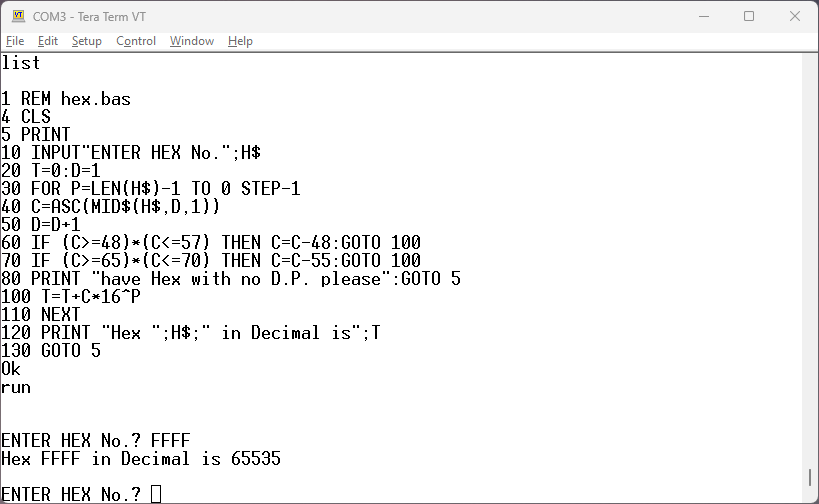
In a MS-Windows editor, you can select the hex.bas
BASIC source code with CTRL-A, copy with CTRL-C and insert into Tera
Term window with ALT-V. Attention: ALT-V, not
CTRL-V.
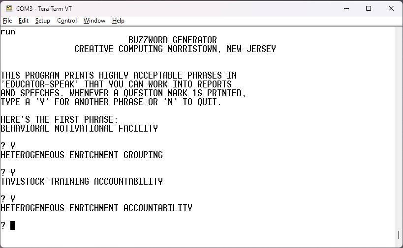
MS-BASIC Buzzword
An important part of advertising and
persuasion are catchy phrases. If you lack in this department,
the program Buzzword.bas helps.
Author was David Ahl in
101
BASIC computer games, Microcomputer Edition.
MS-BASIC NIM
There are three versions of NIM in "101 BASIC computer games,
Microcomputer Edition". The following is 23Matches,
the most simple NIM game in the book.
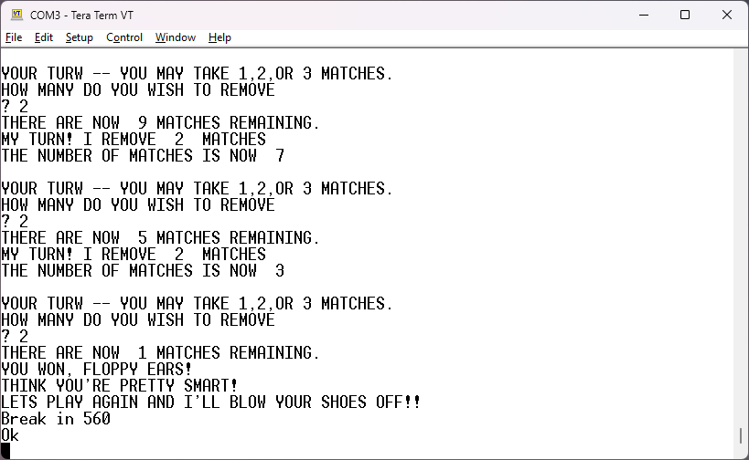
The file is 23MATCH.bas, author is Bob
Albrecht. The game NIM was the Artificial Intelligence craze of the
1940s and 1950s. The Nimatron was an
electro-mechanical machine at the 1939/1940 New York Worlds's Fair.
The Nimrod
was a custom-build computer at the 1951 Festival of Britain. In the
1970s I build a NIM device. The "intelligence" was in the wireing.
Depending on the contact, one to three LEDs lighted for the NIM
move. The Nim game has a very
simple solution. If you reduce the number of matches to
(N*4)+1 in all your moves, you will win 23Matches. Because the
german minister Ludwig
Erhard did not know the trick, he lost against the "electronic
brain" Nimrod.
MS-BASIC Hamurabi
The book "101
BASIC computer games" was published in 1973 by Digital
Equipment Corporation for different BASIC dialects. In 1978 the "101
BASIC computer games, Microcomputer Edition" was published for
Microsoft BASIC 4.0. The game Hammurabi or Hamurabi is a simple city
simulation/strategy game. You are the administrator.
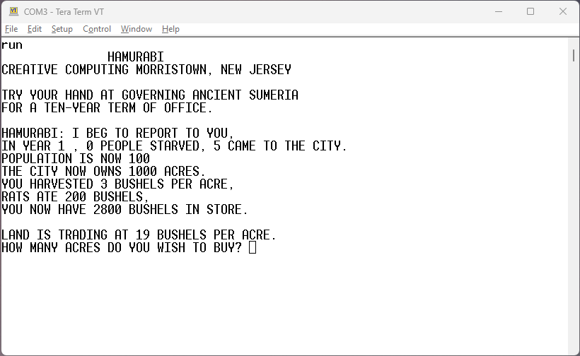
The file is Hamurabi.bas. The original
author of this game is unknown. The first implementation was in FOCAL
programming language.
MS-BASIC
Tic-Tac-Toe
There are two versions of Tic-Tac-Toe
in "101 BASIC computer games, Microcomputer Edition". The first
version plays perfect, but always starts.
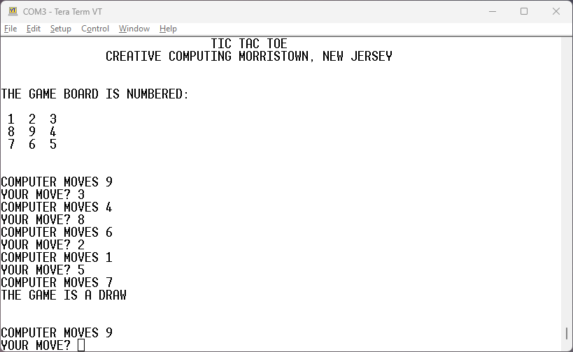
The file is TTT.bas. The original author is
Tom Koos. The program was modified by Steve North.
MS-BASIC Game of
Life
John Conway's "Game
of Life" is no game, it is a cellular automaton or even a
real-life simulation game. "Cells" are "living" on a grid with three
simple rules for birth, survival and death. These three rules result
in an universal Turing machine that can compute anything that your
digital computer can compute. Some implementations of Life start
with random seed. This implementation from Clark Baker and Steve
North starts with user given seed. Interesting seeds are "glider",
"glider gun" or even "breeder".
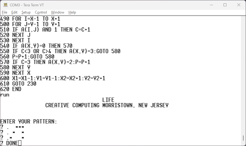
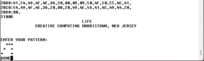
The seed in the screenshot above is shaped like a little N. The
first dot is interpreted as space. The entry "DONE" starts the
simulation.
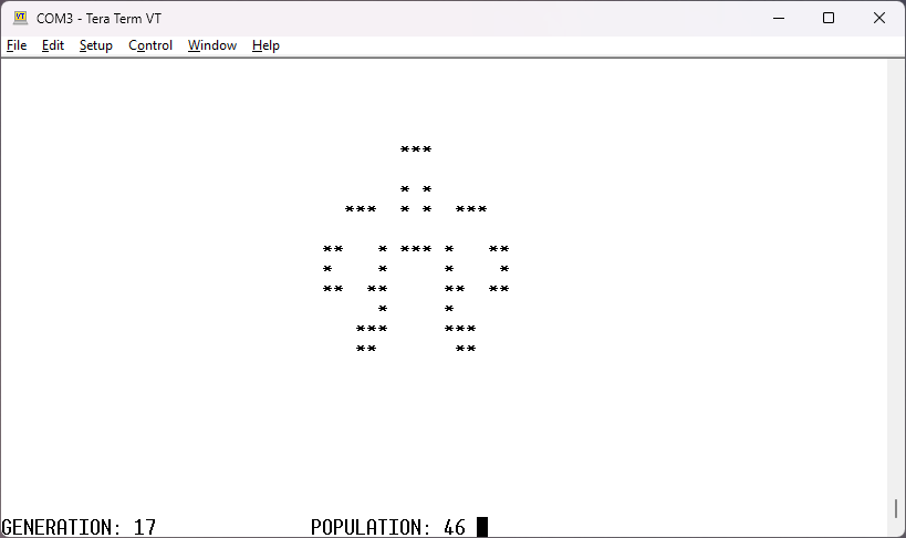
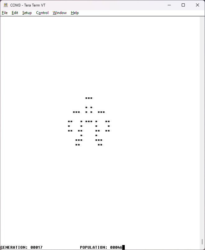
After 17 generations we see a man-shaped figure. After 172
generations the seed becomes a stable oscillating pattern. Most
seeds expand for some generations before still lifes and oscillators
fill the grid. But grow beyond bounds is possible with "glider
guns". The BASIC program is LIFE.bas from 101
BASIC computer games, Microcomputer Edition. I simplified the
BASIC source code and renumbered it. The program executes fine on
DOSbox and GW-BASIC.
Game of Life in C
The BASIC interpreter version using floating point numbers is
slow. The algorithm of the BASIC program is clever. I want to
implement this algorithm in Z80 assembler. There is the straight
forward way from BASIC to assembler. I decided to use a detour via
"superassembler", aka programming language C. The source code is life.c, the MS-Windows execute is life.exe. First I discuss the transcribe of
the BASIC program:
#define XSZ 50 // grid size rows
#define YSZ 70 // grid size columns
#define DD 0 // is death, becomes death
#define LL 1 // is live, becomes live
#define DL 2 // is death, becomes live
#define LD 3 // is live, becomes death
int main()
{
// REM LIFE.bas
char A[XSZ+1][YSZ+1],
B[XSZ+1][40];
// DIM A(26,70),B$(24)
memset(A, 0,
sizeof(A));
// zero A
int C=0, G=0, P=0,
E=0;
// C=0:G=0:P=0:E=0
TAB(34);
printf("LIFE\n");
// PRINT TAB(34);"LIFE"
TAB(15); printf("CREATIVE COMPUTING
MORRISTOWN, NEW JERSEY\n"
"\n\n"
"ENTER YOUR PATTERN:\n");
for (;;)
{
// L80:
fgets(B[C],
sizeof(B[0]),
stdin);
// INPUT B$(C)
*strchr(B[C],
'\n')='\0';
// remove \n
if (strstr(B[C],
"DONE"))
{
// IF B$(C)="DONE" THEN
break;
// L110
}
++C;
// C=C+1
}
// GOTO L80
// L110:
--C; unsigned
L=0;
// C=C-1:L=0
for(int X=0; X<=C-1; ++X)
{
// FOR X=0 TO C-1
if
(strlen(B[X])>L)
// IF LEN(B$(X))>L THEN
L=strlen(B[X]);
// L=LEN(B$(X))
}
// NEXT X
int X1=XSZ/2-C/2,
X2=X1+C;
// X1=13-INT(C/2):X2=X1+C
int Y1=YSZ/2-L/2,
Y2=Y1+L;
// Y1=35-INT(L/2):Y2=Y1+L
for (int X=0; X<=C; ++X)
{
// FOR X=0 TO C
for (unsigned Y=0;
Y<strlen(B[X]); ++Y)
{
// FOR Y=1 TO LEN(B$(X))
if (B[X][Y]=='*')
{
// IF MID$(B$(X),Y,1)="*" THEN
A[X1+X][Y1+Y]=1;
++P;
// A(X1+X,Y1+Y)=1:P=P+1
}
}
// NEXT Y
}
// NEXT X
printf("\n\n");
// PRINT:PRINT
The two #define tell the grid size in X and Y direction. XSZ
is number of rows, YSZ is number of columns. The complete BASIC
program is one function (subroutine, procedure), therefore
everything is in C language function main(). The first part is
enter the seed formation. The BASIC GOTO statements are replaced
by structured elements of C. The GOTO 80 is replaced by a
"forever" loop. The GOTO 110 is replaced by "break", the
structured loop exit.
for(;;)
{
// L230:
int X4=2, X3=XSZ-2,
Y4=2,
Y3=YSZ-2;
// X4=2:X3=24:Y4=2:Y3=68
for (int X=1;
X<=X1-1; ++X)
printf("\n");
// FOR X=1 TO X1-1:PRINT:NEXT X
printf("\n");
// BASIC FOR-NEXT at least loops once
for (int X=X1;
X<=X2; ++X)
{
// FOR X=X1 TO X2
TAB(Y1);
// PRINT TAB(Y1);
for (int Y=Y1; Y<=Y2; ++Y)
{
// FOR Y=Y1 TO Y2
if (A[X][Y]==DD || A[X][Y]==LD)
{
// IF A(X,Y)=0 OR A(X,Y)=3 THEN
A[X][Y]=DD; printf(" "); continue;
// A(X,Y)=0:PRINT " ";:GOTO
L340
}
A[X][Y]=LL;
printf("*");
// A(X,Y)=1:PRINT "*";
if (X<X3)
X3=X;
// IF X<X3 THEN X3=X
if (X>X4)
X4=X;
// IF X>X4 THEN X4=X
if (Y<Y3)
Y3=Y;
// IF Y<Y3 THEN Y3=Y
if (Y>Y4)
Y4=Y;
// IF Y>Y4 THEN Y4=Y
// L340:
}
// NEXT Y
printf("\n");
// PRINT
}
// NEXT X
for (int X=X2+1;
X<=XSZ-1; ++X)
printf("\n"); // FOR X=X2+1
TO 24:PRINT:NEXT X
printf("\n");
// BASIC FOR-NEXT at least loops once
printf("GENERATION:
%d\t\tPOPULATION: %d ", G, P); // PRINT
"GENERATION:";G,"POPULATION:";P;
if (E)
printf("INVALID %d",
E);
// IF E THEN PRINT "INVALID";E;
if (P==0)
break;
// IF P=0 THEN STOP
sleep(1);
// slow down computer
The second part prints the grid and determines the "active
grid area". The old area is limited by points X1, Y1 and X2,
Y2. Two nested for() loops walk the active grid. The cell
coding is this:
DD=0 is death, becomes death
LL=1 is live, becomes live
DL=2 is death, becomes live
LD=3 is live, becomes death
A DD cell is printed as space, a LD cell is changed to DD cell and
printed as space, too. The remaining cells (LL, DL) are changed to
LL cell and printed as star. The new active grid is limited by X3,
Y3 and X4, Y4. First these variables are set to minimum (X4, Y4)
or maximum values (X3, Y3). Then these values are changed
depending on the new grid.
X1=X3; X2=X4;
Y1=Y3; Y2=Y4; ++G; P=0;
E=0; //
X1=X3:X2=X4:Y1=Y3:Y2=Y4:G=G+1:P=0:E=0
if (X1<2) { X1=2;
E=1;
}
// IF X1<2 THEN X1=2:E=1
if (X2>XSZ-2) {
X2=XSZ-2; E+=2;
}
// IF X2>24 THEN X2=24:E=2
if (Y1<2) { Y1=2;
E+=4;
}
// IF Y1<2 THEN Y1=2:E=3
if (Y2>YSZ-2) {
Y2=YSZ-2; E+=8;
}
// IF Y2>68 THEN Y2=68:E=4
for (int X=X1-1;
X<=X2+1; ++X)
{
// FOR X=X1-1 TO X2+1
for (int Y=Y1-1; Y<=Y2+1; ++Y)
{
// FOR Y=Y1-1 TO Y2+1
C=0;
// C=0
for (int I=X-1; I<=X+1; ++I)
{
// FOR I=X-1 TO X+1
for (int J=Y-1; J<=Y+1; ++J)
{
// FOR J=Y-1 TO Y+1
if
(A[I][J]&1)
// IF A(I,J) AND
1 THEN
++C;
//
C=C+1
}
// NEXT J
}
// NEXT I
if (A[X][Y]==DD) goto
L570;
// IF A(X,Y)=0 THEN L570
if (C<3 || C>4)
{
// IF C<3 OR C>4 THEN
A[X][Y]=LD;
continue;
// A(X,Y)=3:GOTO L580
}
++P;
continue;
// P=P+1:GOTO L580
L570:
// L570:
if(C==3)
{
// IF C=3 THEN
A[X][Y]=DL;
++P;
// A(X,Y)=2:P=P+1
}
// L580:
}
// NEXT Y
}
// NEXT X
--X1; --Y1; ++X2;
++Y2;
// X1=X1-1:Y1=Y1-1:X2=X2+1:Y2=Y2+1
}
// GOTO L230
}
// END
The third part is "pruning" the new grid size. First the new
active grid is copied from (X3, Y3, X4, Y4) to (X1, Y1, X2, Y2).
Then values are limited. The "INVALID" number E is calculated.
Next are four nested loops. The X and Y loops iterate over the
active grid. The I and J loops iterate over the neighbors and the
cell itself. Because the cell is included, the "die" condition is
now a C value of less then 3 or more then 4. To allow "birth" at
the border of the active grid, X1, Y1 and X2, Y2 are expanded one
step outwards. Only one GOTO remains in the C source code. The
"continue" key word starts the next loop iteration. Some purists
have problems with "break" and "continue". I think they are
valuable structured(!) elements.
Game of Life, C
pointer version
The array operations like A[I][J]==1 are transcribed to pointer
operations like *pJ==1. These pointer operations are easy to code
in assembler. The C source file is life2.c,
the MS-Windows execute is life2.exe. I
show the third part with four nested loops as example:
X1=X3; X2=X4;
Y1=Y3; Y2=Y4; ++G; P=0; E=0;
if (X1<2) { X1=2;
E=1; }
if (X2>XSZ-2) {
X2=XSZ-2; E+=2; }
if (Y1<2) { Y1=2;
E+=4; }
if (Y2>YSZ-2) {
Y2=YSZ-2; E+=8; }
pX=&A[X1-1][0];
for (int X=X1-1;
X<=X2+1; ++X, pX+=(YSZ+1)) {
char* pY=pX+Y1-1;
for (int Y=Y1-1; Y<=Y2+1; ++Y, ++pY) {
C=0;
char* pI=pY-(YSZ+1);
for (int I=X-1; I<=X+1; ++I, pI+=(YSZ+1)) {
char* pJ=pI-1;
for (int J=Y-1; J<=Y+1; ++J, ++pJ) {
if (*pJ&1)
++C;
}
}
if (*pY==DD) goto L570;
if (C<3 || C>4) {
*pY=LD; continue;
}
++P; continue;
L570:
if(C==3) {
*pY=DL; ++P;
}
}
}
--X1; --Y1; ++X2;
++Y2;
There two inner I and J loops can be unrolled for even more
speed.
Game of Life, C
unrolled version
Optimizing the inner loops brings best benefits. Unrolling is
repeating the loop action again and again. The C source file is life3.c, the MS-Windows execute is life3.exe. I show the third part with
unrolled I and J loop as example:
for (int X=X1-1;
X<=X2+1; ++X, pX+=(YSZ+1)) {
char* pY=pX+Y1-1;
for (int Y=Y1-1; Y<=Y2+1; ++Y, ++pY) {
C=0;
char* p=pY-(YSZ+1)-1; if (*p&1) ++C;
++p; if (*p&1) ++C;
++p; if (*p&1) ++C;
p+=(YSZ+1); if (*p&1) ++C;
--p;
--p; if (*p&1) ++C;
p+=(YSZ+1); if (*p&1) ++C;
++p; if (*p&1) ++C;
++p; if (*p&1) ++C;
if (*pY==DD) goto L570;
if ((C<2) || (C>3)) {
*pY=LD; continue;
}
++P; continue;
L570:
if(C==3) {
*pY=DL; ++P;
}
}
}
--X1; --Y1; ++X2;
++Y2;
The unrolled version makes it easy to test only the eight neighbors.
The expression (*p&1) returns the values 0 or 1. These values
can be added to variable C to calculate the number of neighbors.
Avoiding if (conditional) is a good thing (TM). The
unrolled version can be used with a Z80 C language compiler like the
HI-TECH
Z80 C Cross Compiler for MS-DOS. Or the C source code is
transcribed by hand to assembler.
Game of Life, C
intermediate version
Another step on the way to Game of Life in Z80 assembler is
converting the C source code to the peculiarities of HI-TECH Z80 C
cross compiler and do away with LIBC functions. The HI-TECH allows
only old-style /* */ comments. Next, variable definitions have to
come first in a function. The LIBC function printf() is replaced by
cputs(), a function to print C-string constants and prbcdu(), a
function to print unsigned 16-bit numbers. The fgets() function is
replaced by sgets(). Note: Never use a input function like gets()
that has no length-check of input. The functions cputs() and sgets()
use single character functions putch() and getche(). These functions
calls the monitor subroutines.
The intermediate version life4.c compiles on
the HI-TECH Z80 C cross compiler in DOSbox and compiles on
Code::Blocks with GNU GCC compiler on MS-Windows 11. It runs on
MS-Windows, but does not run on Z80 computer with monz80.
Game of Life, C
monz80 version
The functions putch() and getche() need monz80 versions for my Z80
computer:
void putcm(char c) {
#asm
ld a,(ix+4)
rst 08h
#endasm
}
static char c_;
void getcm(void) {
#asm
rst 10h
ld (_c_),a
#endasm
}
void putch(char c) {
if(c == '\n')
putcm('\r');
putcm(c);
}
char getche(void) {
getcm();
if (c_ == '\r')
c_='\n';
putch(c_);
return c_;
}
The functions putcm() and getcm() contain the monitor calls. The rst
08h monitor call outputs a character in A register, rst 10h reads
keyboard input into register A. The #asm and #endasm preprocessor
directives are HI-TECH C compiler specific. The putch() and getche()
functions realize "cooked
terminal mode". For output, the '\n' is converted to "\r\n".
For input, the '\r' is converted to '\n' for the program and "\r\n"
for the terminal.
The output of life5.c is like life.bas. As
little difference, the prbcdu() function prints leading zeros. A key
entry like SPACE creates the next generation.
The binary file life5.bin is converted to life5.mon which can be downloaded to Z80
computer and started with 2100R:
Game of Life,
monz80 hand-optimized
Let's look at the compiler assembler output of the inner loops:
;life4.c:
148:
C=0;
ld (ix+-1),0
;life4.c:
149:
p=pY-(70 +1)-1; if (*p&1) ++C;
ld de,(_pY)
ld hl,-72
add hl,de
ld (_p),hl
bit 0,(hl)
jp z,l88
inc (ix+-1)
;life4.c:
150:
++p; if (*p&1) ++C;
l88:
ld hl,(_p)
inc hl
ld (_p),hl
bit 0,(hl)
jp z,l89
inc (ix+-1)
;life4.c:
151:
++p; if (*p&1) ++C;
l89:
ld hl,(_p)
inc hl
ld (_p),hl
bit 0,(hl)
jp z,l90
inc (ix+-1)
;life4.c:
152:
p+=(70 +1); if (*p&1) ++C;
l90:
ld de,71
ld hl,(_p)
add hl,de
ld (_p),hl
bit 0,(hl)
jp z,l91
inc (ix+-1)
;life4.c:
153:
--p;
l91:
ld hl,(_p)
dec hl
ld (_p),hl
The variable C is a local or stack variable and index register IX is
used to access this variable. The pointer variables _pY and _p are
static (global) variables. Note: on simple CPUs like Z80, access of
static variables is faster then access of local variables. I say,
the HI-TECH optimizer is doing a good job, but there are miles to
go. The inner loop only uses registers HL and DE for pointer
calculation. Register C is free to be used as register variable C.
Next, there is no need to write HL to variable _p and read it back.
The hand-optimized assembler code is therefore:
;life4.c:
148:
C=0;
ld c,0
;life4.c:
149:
p=pY-(70 +1)-1; if (*p&1) ++C;
ld de,(_pY)
ld hl,-72
add hl,de
bit 0,(hl)
jp z,l88
inc c
;life4.c:
150:
++p; if (*p&1) ++C;
l88:
inc hl
bit 0,(hl)
jp z,l89
inc c
;life4.c:
151:
++p; if (*p&1) ++C;
l89:
inc hl
bit 0,(hl)
jp z,l90
inc c
;life4.c:
152:
p+=(70 +1); if (*p&1) ++C;
l90:
ld de,71
add hl,de
bit 0,(hl)
jp z,l91
inc c
;life4.c:
153:
--p;
l91:
dec hl
Optimizing other parts of the program won't bring much "return of
investment". The assembler file life6.as
started as C compiler assembler output of life5.c. The download file
is life6.mon.
to be continued ...
Palo Alto Tiny
BASIC
Li-Chen Wang created a Tiny BASIC for Intel 8080 that is well known
for the "COPYLEFT ALL WRONGS RESERVED" comment in the source code.
The "PCC's Reference Book of Personal and Home computing" contains Palo
Alto Tiny BASIC Version Three. The version 3 fixed some bugs
and did not use the RST opcodes (RST use conflicts with my monz80).
The assembler listing uses two assembler macros TSTC and ITEM that
are not defined in the article. Using the listing and the TASM
manual I reverse engineered the macros for TASM assembler:
#define ITEM(s,a) .text
s\ .byte
(a>>8)|80h,a&0FFh
#define TSTC(c,a) call
TSTCH\ .text
c\ .byte a-*-1
As often, macros do not accept all ASCII characters. The TASM allows
octal coding of characters. Therefore you sometimes see
TSTC("\054",LS1) ; ,
The octal ASCII code of comma is 054.
The assembler source is TB.asm. The download
file for monz80 is tb.mon. Load tb.mon into an
ASCII text editor, select all with CTRL-A, copy with CTRL-C and
paste into Tera Term with ALT-V. Start Tiny BASIC with F000R.
The screenshot shows PATB (Palo Alto Tiny BASIC). This Tiny BASIC
has FOR-NEXT loops, multiple commands in one line and one
one-dimensional array @(). The BASIC program rndtst.bas
shows the low quality of the RND() function.
PATB Mandelbrot
Gordon Henderson wrote Retro
Basic Benchmarking with Mandelbrot. I ported the 16-bit
integer Mandelbrot program from BBC BASIC to PATB. "Computed" GOTO
is used as alternative to MID$().
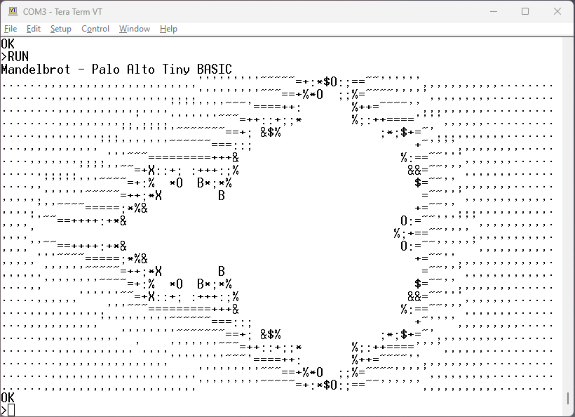
The file is mandelb.bas. Tiny BASIC does
not used 1-byte tokens for PRINT and GOTO. You can use P. for PRINT
and G. for GOTO to save some memory.
Note: The BAS file contains eight DEL characters per line. These superfluous
characters give the BASIC interpreter time to store the BASIC
line into memory.
PATB Tic-Tac-Toe
There is a Tic-Tac-Toe
game for Tom Pittman's Tiny BASIC for 6502, 6800 computer. I
ported it to Palo Alto Tiny BASIC.
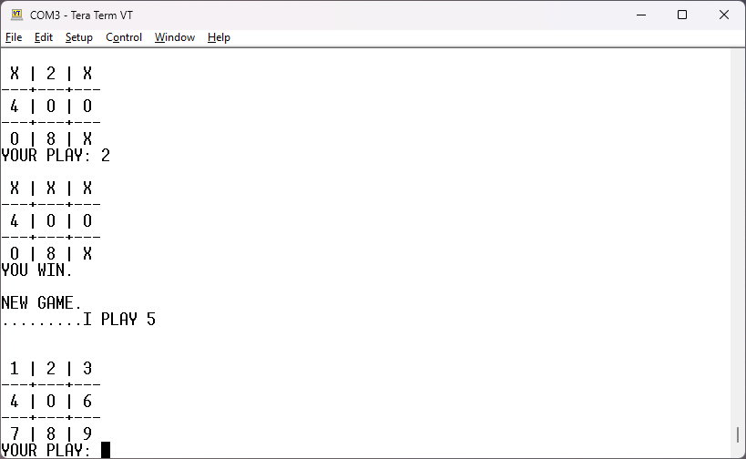
The file is tictact.bas. The
algorithm has a weakness. You win by playing 1, 9, 3, 2.
NASCOM computer
The NASCOM 1 was
an UK computer kit from 1977 with a keyboard and video output to
television with 48 columns and 16 rows. Like the Tandy Radio Shack
TRS-80 it was an early "home computer". The magazine Wireless
World, november 1977, has the article "Microcomputer design"
by Phil Pittman with a NASCOM 1 advertisment:
"This kit, known as NASCOM 1, includes a Mostek Z80 microprocessor,
MK3880; 2Kbyte of r.a.m. using Mostek 1024-bit r.a.ms, MK4102;
1Kbyte of e.p.r o.m. using the Mostek 1024x8-bit e.p.r.o.m. MK2708;
u.a.r t. type IM6402; character generator MCM6571A; i.cs. for video
r.a.m. logic; zener diodes; 16MHz crystal; interfaces; a keyboard;
and p.c. boards. Price £197.50 (ex. v.a.t.).
The microcomputer is designed to use a domestic tv set as a visual
display and a standard audio cassette tape recorder for programme
storage."
NASCOM emulator
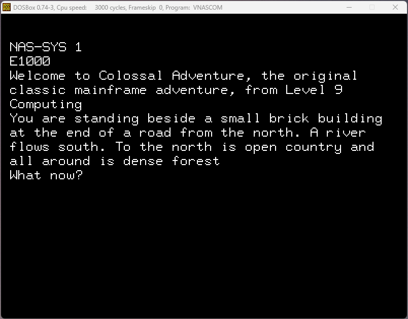
VNASCOM
The Nascom Home Page by
Tommy Thorn and Constantin Olbrich has Virtual
Nascom Version 3.1 for DOS/Win9x/ME, a MS-DOS NASCOM emulator
that executes in DOSbox. 64-bit MS-Windows executes 16-bit MS-DOS
executes 8-bit Z80. Put your Giga-Hertz computer to good use. In the
Games section I found Colossal
Adventure (32K) by Level 9 with Solution.
First start DOSbox. Then start VNASCOM with
VNASCOM RAM=ADVENTR.NAS TRA=GER KBD=E1000
Note: TRA=GER is only needed for german keyboard layout.
Colossal
Cave Adventure by Will Crowther (and Don Woods) was the first
computer adventure game. First
implementation was 1976 on a PDP-10 in Fortran. The Digital
Antiquarian tells us that Level 9, or the Austin brothers,
released their version of Colossal Adventure in early 1982 for
NASCOM. Level 9 used sophisticated compression to squeeze 200 rooms
into 32 KByte. The disadvantage is slow text output. Jimmy Maher
concludes "That’s not, however, to say that I can really recommend
them to players today". In my opinion, the NASCOM computer is cult
and Colossal Cave adventure is cult, too. Armed with a solution, I
happily enter the cave!
More information like details of the text parser is in the Level 9
manuals Jewels
of Darkness on ifarchive.org.
to be continued ...
Intel hexadecimal
object file format
The early Intel development systems Intellec 4 (4004, 4040) and
Intellec 8 (8008, 8080) had no mass storage. The "computer terminal"
of the day was an electromechanical teletype like the ASR 33.
The paper tape read and punch unit of the teletype provided the
first mass storage. The ASR-33 used 7-bit ASCII, but implemented
only upper case letters. The Intelhex format uses two ASCII
characters to encode one byte. At the 20mA current loop interface
the ASR-33 used a parity bit to allow error detection. The paper
tape had no parity bit track. Therefore Intelhex uses a checksum
byte for error detection.
Intelhex record type 00 and 01 were defined in 1973. Other record
types were added for 8086 and later microprocessors.
PL/M-80
Gary Kindall invented the programming language PL/M and the
operating system CP/M. In 1975 one could choose between the
programming languages Pascal, PL/M and C. Only C is in use today.
Pascal was used to teach students structured programming. PL/M was
used to write the single-user/single-task operating system CP/M. C
was used to write the multi-user/multi-task operating system UNIX.
Pascal and C allow recursive functions. PL/M functions are not
recursive by default. This is a good optimization feature for the
Intel 8080 that has no efficient stack-relative addressing modes.
The REENTRANT attribute makes a PL/M function recursive. The
implementation of the strcpy() function shows the power and elegance
of C. Here is the ANSI-C version:
void strcpy(char *d, char *s)
{
while(*d++ = *s++)
;
}
The PL/M version is:
STRCPY: PROCEDURE (D, S);
DECLARE (D, S) ADDRESS,
(DI BASED D, SI BASED S)
BYTE;
LOOP: DI = SI;
S = S + 1;
D = D + 1;
IF DI <> 0 THEN GOTO LOOP;
END STRCPY;
The GOTO statement is needed because there is no do..while loop in
PL/M. Pointer arithmetic in PL/M is strange for a C programmer.
There is no dereference operator in PL/M, one has to create a
variable that is BASED on the pointer variable for indirection. Like
Pascal, PL/M allows nested procedures. The CP/M sources make very
little use of nested procedures. The author wonders: Structured
programming with nested blocks were a great invention in computer
science. Did some people think that nested procedures were even
better?
The 8080 microprocessor can handle three pointers in registers. The
H, L register pair is more flexible than the B, C or D, E register
pair. All "pointer registers" allow to load and store the
accumulator from the pointer address. One implementation of the
strcpy() function in 8080 assembler is:
LOOP: LDAX B
STAX D
INX B
INX D
JNZ LOOP
The pointer s is in registers B, C and the pointer d is in registers
D, E.
PL/M Parameter
passing conventions
The strcpy() function above uses two parameters. One method of
parameter passing is to use the stack. The calling function puts the
values of argument 1 and argument 2 on the stack, the called
function gets the parameter off the stack. This method allows
recursive functions. Another method is to pass arguments in
registers. A third method is to have "hidden" global variables for
parameter passing. The second and third method do not allow
recursive functions. The Intel "A Guide to PL/M Programming"
document from September 1973 tells in section "Subroutine linkage
conventions" how parameter passing is done on a PL/M 8008 system.
The first argument is passed in registers B, C. The second argument
is passed in registers D, E. Additional parameters are passed as
"hidden" global variables. Strange for me, the author, is the
convention to pass low byte in register B or D and high byte in
register C or E. The 8080 microcomputer has 16-bit addition opcodes.
These opcodes require low byte in registers C, E or L and high byte
in registers B, D or H.