Andre Adrian, DL1ADR, 2026-04-07
After the 6800 8-bit data bus microprocessor and before the 68000
16-bit data bus microprocessor, Motorola produced the 6809
8-bit data bus microprocessor. Some say the 6809 was the best
8-bit micro, others say the 6809 was too late and expensive, 6502
and Z80 were too much of competition. The 6809E (external clock)
was the CPU in the Tandy Color Computer from 1980 and the Dragon
32, Dragon 64 computers. The 6809 uses a single clock input, the
6809E uses two clock inputs E and Q that have a phase difference
of 90° (in-phase and quadrature clock). The Motorola 6883 (SAM)
dynamic RAM controller uses the E and Q clocks to "steal" memory
cycles from the CPU for video display or DRAM refresh.
Hitachi produced the 6309 as
CMOS version of the NMOS 6809. The HD63C09EP is easy and cheap to
find. This is one reason I chose this microprocessor. The more
important reason is the Hirotsugu Kakugawa document "A
MEMO ON THE SECRET FEATURES OF 6309" from 1992. According to
this paper, the 6309 has LOTS of useful undocumented opcodes. "The
6309 Book" from Chris Burke explains these features in
detail. Highlights are hardware 16-bit * 16-bit multiplication and
hardware 32-bit / 16-bit division that use 32-bit accumulator Q.
Grant Searle has a 6-chip
6809 computer with a tailored MS-BASIC. Jeff Tranter has a 6809
Single Board Computer with PCB. Jeff has 6809 software,
including a ported Wozmon, on his 6809 github page.
Tom LeMense has a sophisticated
6309 computer with SMD parts.
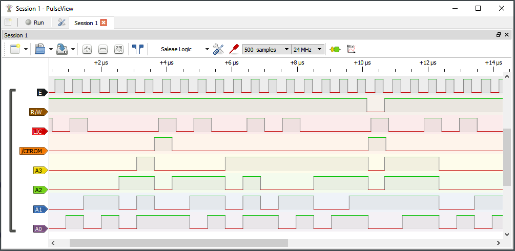
I test the 6309E with a NOP tester, that is minimum hardware to
run the NOP opcode. A little 8-channel logic analyzer shows the
correct working of the microprocessor and the clock logic.
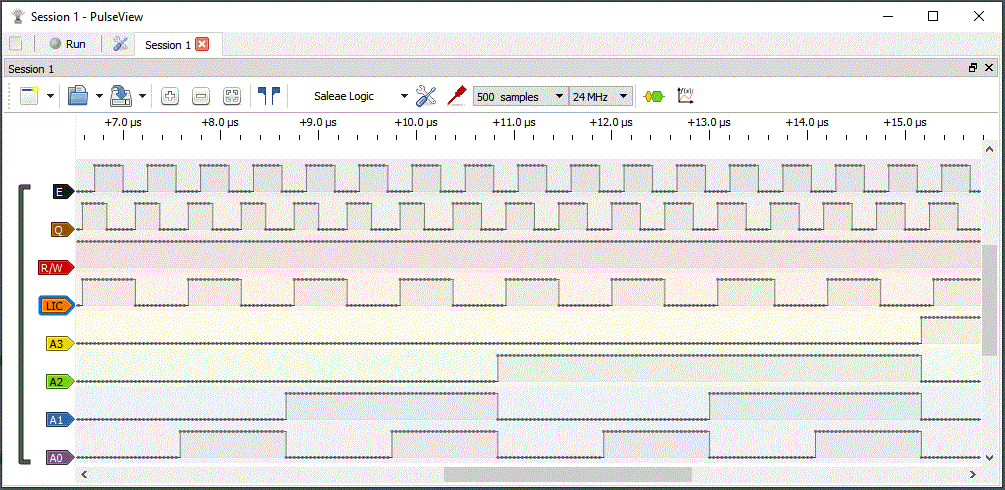
The NOP opcode ($12) uses two cycles. The LIC (Last Instruction
Cycle) happens once for every opcode. Like with the 2650, NOP is a
"slow" opcode. One cycle is used for opcode fetch, the second
cycle does nothing.
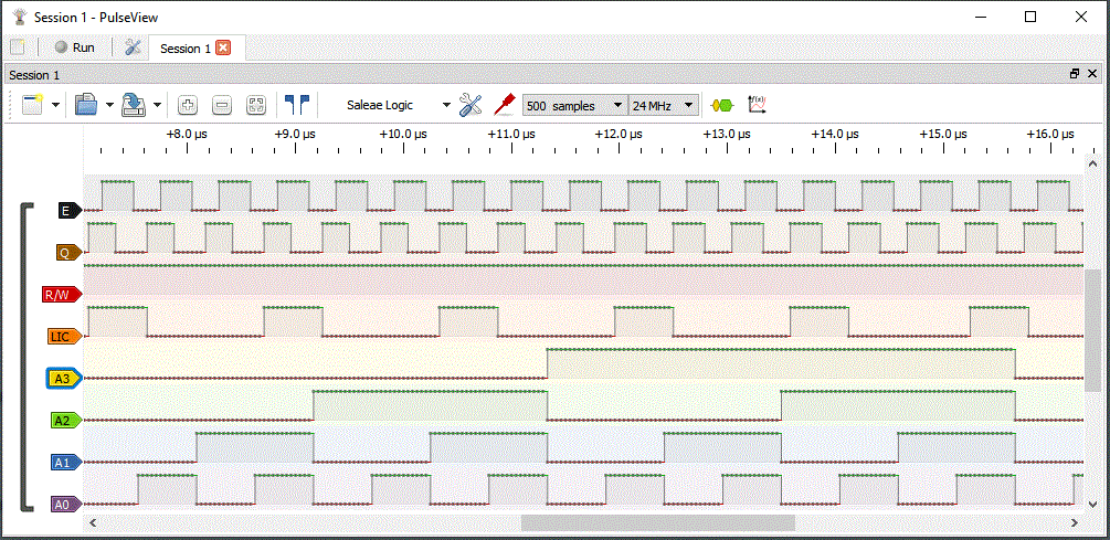
The LDD immediate ($CC) opcode uses three cycles. First fetches
opcode, second and third fetch the 16-bit immediate value to load
into accumulator D. Every cycle performs a memory-read operation,
therefore LDD is a "fast" opcode. Every three cycles a LIC cycle
happens.
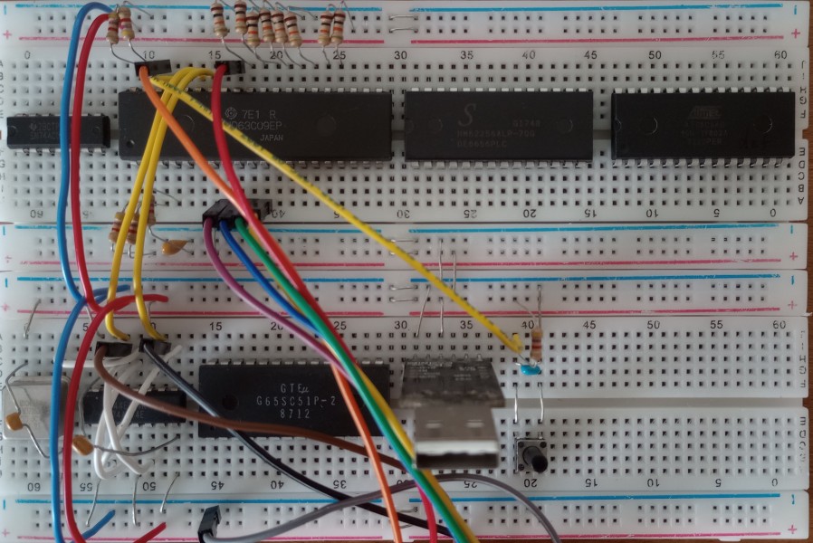
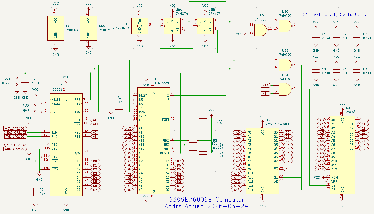
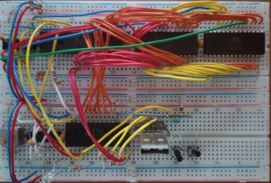
On the two breadboards, all 6 chips are already in place. Upper
breadboard has glue-logic 74HC00, CPU 6309E, RAM 62256 and ROM
28C64. Lower breadboard has quartz oscillator 7.3728 MHz, 74HC74,
ACIA 65C51, USB-to-UART PCB with CP2102 and reset push button.
Only the oscillator, the clock generator 74HC74 and the CPU are
wired. The 8 10 kOhm resistors at the top are set on $CC (LDD)
opcode.
The CPU pins 2 /NMI, 3 /IRQ, 5 /FIRQ, 37 /RES and 40 /HALT are
connected via individual 4.7 kOhm resistors to VCC (+5V). Pin 39
TSC is connected via 4.7 kOhm to GND (0V).
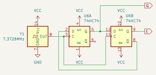
The E, Q in-phase and quadrature clocks are created with two D
flip-flops in the 74HC74. The Hitachi HD63C09E datasheet uses JK
flip-flops, but D flip-flops are easier to get.
The Motorola 68xx series has the 6850 as ACIA (Asynchronous
Communications Interface Adapter). This chip is hard to find and
not available in CMOS. I prefer the MOS Technology 65C51. I used
the WDC65C51 with "special needs", aka documented bugs, in the 65C02
computer. This time I use a GTE G65SC51P-2, the 2MHz
version of the ACIA, with production date
8712. The idea is to use 19200 bps (bit per second)
without handshake. RTS/CTS hardware handshake is wired.
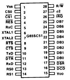
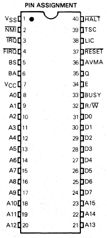
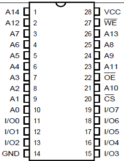
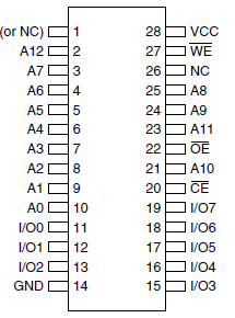
IC pinout: 65C51, 6309E, 62C256, 28C64:
 |
 |
 |
 |
The clock generator with Y1 quartz oscillator and U6 74HC74 was
discussed above. The glue logic with U5 is the same as with 65C02
computer. The chip select uses address bus A15 and A14. If A15 is
low, RAM is selected because A15 is connected to /CE of RAM. If
A15 is high and A14 is low, U4 65C51 ACIA is selected, because A15
and A14 are connected to CS1 and /CS2. If A15 and A14 are high,
the NAND gate U5A output is low and U3 28C64 ROM is
selected.
RAM address range is from $0000 to $7FFF. ACIA address range is
$8000 to $8003 with a lot of duplicates up to $BFFF. ROM address
range is $E000 to $FFFF with a duplicate in $C000 to $DFFF.
I use the LWTOOLS from
William Astle, an assembler (lwasm), linker (lwlink) and library
tool (lwar). MS-Windows
binaries are available. The assembler uses "CUI", character
user interface or command line. I start "cmd", the command line
program, with Windows-key R.
The 6309 computer has a push button on the /DSR input of the
65C51 and a LED at the /RTS output. The first program uses this
primitive IO. While you press the button, the LED shall light. The
important part of the assembler program first.asm
is:
forever:
; for(;;) {
LDB
#$02
; B = RTS_High
LDA ACIA_STATUS
; A = ACIA_STATUS
ANDA
#$40
; A &= DSR_MASK
BNE
endif
; if (A != 0) {
LDB
#$0A
; B = RTS_Low
endif:
; }
STB
ACIA_CMD ;
ACIA_CMD = B
BRA
forever ; }
Accumulator B is used for the output value to the 65C51.
Accumulator A is used for the input from 65C51.
The command to create a BIN file for ROM programming out of ASM
file:
lwasm -r first.asm -ofirst.bin -lfirst.lst
You can use first.bin to program the
28C64. I use a TL866II Plus as ROM programmer.
The Logic Analyzer shows the running program as no button is pressed. The forever loop starts at address $xxx0 and has the BRA opcode on $xxxE and $xxxF. The first.lst file shows the details of the program. The important part is:
E000
forever:
; for(;;) {
E000
C602
LDB
#$02
; B = RTS_High
E002
B68001
LDA ACIA_STATUS
; A = ACIA_STATUS
E005
8440
ANDA
#$40
; A &= DSR_MASK
E007
2602
BNE
endif
; if (A != 0) {
E009
C60A
LDB
#$0A
; B = RTS_Low
E00B
endif:
; }
E00B
F78002
STB
ACIA_CMD ;
ACIA_COMMAND = B
E00E
20F0
BRA
forever ; }
The first column is the program address, the second column is the
opcode. Note: The 6809E fetches always the next byte from program
memory if there is nothing better to do. The STB ACIA_CMD opcode
has 3 bytes opcode plus one memory write but extends over 5 E
clocks. The fourth E clock performs an "empty" memory read of
address $FFFF.
The complete 6309E computer. Left push button is reset, right is
input. Press input button and LED lights. We build a simple light
switch with a microprocessor! While you press reset, LED lights,
too.
The monitor program or BIOS program allows the computer to use
the serial interface. Typically you can display memory contents,
change memory contents and download programs into the 6309
computer. The monitor programs grew in size: Apple 1 6502 Wozmon
is 256 Bytes, Motorola
6800 MIKBUG is 512 Bytes, Signetics 2650 PIPBUG is 1 KByte
and SWTPC
6809 SBUG is 2 KByte. Note: The Southwest Technical Products
Corporation (SWTPC) developed and sold kits. For Motorola 6800 it
was like ALTAIR and IMSAI for Intel 8080 (or better).
Some years ago I developed a small monitor for 65C02, mon65C02.asm. I ported this 65C02
program to 6309 for a 256 bytes "Wozmon like" monitor. The monitor
uses only 2 bytes in the direct page at address $0000 to $0001.
The monitor prompt is \ (backslash).
To print memory area FF00 to FFFE enter:
FF00:FFFEP
To enter values into memory, starting at address 0x200, enter:
200:11,2,AF,
The values are 0x11, 0x02, 0xAF. After EVERY byte a , (comma) is
needed.
To start a program at address 0xFF00 enter:
FF00R
Lower case characters are converted to upper case. There is no
input line and therefore no line editing.
About the mon6309 language: minimum state and postfix. States are
necessary if something from the past is needed to handle the
present. For example, in LET B=A+1 the expression A+1 is part of
an assign, in IF B>A+1 the same expression is part of a
compare. Postfix is NOUN VERB, that is first the object, then the
action. The NOUN in the mon6309 language is a hexadecimal number
of 1 to 4 digits, like 0, 19, AFFE or BA9. The VERBS are:
: to store the NOUN as 16-bit address in argA
, to store the NOUN as 8-bit value at address argA and increment
address argA
P to print the contents of the address range from argA to NOUN
R to run the program at address NOUN
CR (carriage return) to print CR, LF and the prompt
The monitor is mon6309.asm, as a 8
KByte binary file mon6309.bin. The 6309
version has argA in register X or D.
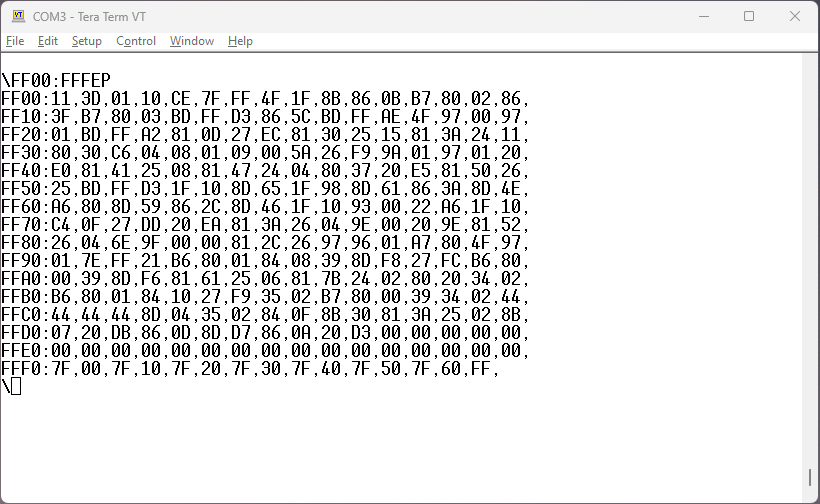
Tera Term screenshot with mon6309 Hex listing.
The conversion from 65C02 assembler to 6809/6309 assembler was
mostly straight forward, but I found these road blocks:
Note: The 6809 accumulator D is like a 68000 D register and the
registers X, Y are like A registers. Indexed address mode is only
possible with X, Y. 16-bit compare is only possible with D. There
are only very few register-register opcodes with the 6809, the
6309 fixes this. Typical for 6809 is to put values on stack
instead to put values in registers.
The BIOS has the following "operating system" subroutines:
$FF00 reset, start mon6809
$FF94 keybd, return input character available if register A
!= 0
$FF9A getc, return input character in register A
$FFAE putc, print output character in register A as ASCII
$FFBD putbyte, print output character in register A as
hexadecimal
$FFD3 putcrlf, print carriage return, line feed
The 6309 computer uses 7n1, that is one stop bit. The Terminal
emulator uses 2 stop bits. This little difference gives the 6309
computer more time to process the download.
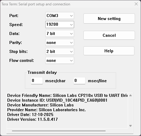
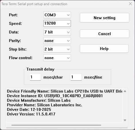
The Tera Term Terminal setup is simple:
Don't forget to Save Setup of Tera Term:
At the page Some
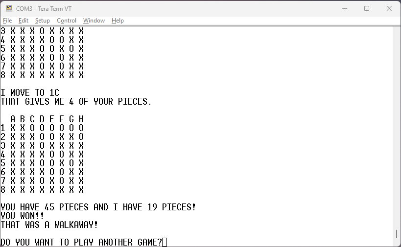
6800 programs from Daniel Tufvesson, I found Othello, an
Othello game program in 6800 assembler. I ported this program to
6309 assembler and adapted it to mon6809a BIOS. This program plays
much faster then the Othello
game in MicroWorld BASIC for the 2650. I assume one Othello
game is the port of the other.
To play the game, download Othello6309.mon
to the 6309 computer. Open the Mon file with an text editor,
select all with CTRL-A, copy with CTRL-C and paste into Tera Term
with ALT-V. Then start the program with 100R. The source
code is Othello6309.asm.
The 6809 does not have some of the register-register 6800
opcodes, but the 6309 has. See the following table:
6800 6309
ABA ADDR
B,A A += B
CBA CMPR
B,A compare A-B
TAB TFR
A,B B = A
TBA TFR
B,A A = B
TSC Micro BASIC from Technical Systems Consultants from 1976 is
an odd beast: An integer BASIC using BCD numbers. The user
manual with source code listing is on Michael Holley's SWTPC
6800/6809 documentation collection. Jeff Tranter ported this 6800
program to 6809
TSC Micro BASIC for his 6809
Single Board Computer. The source code file tscbasic6809.asm is my port to my
6309 computer with mon6809 monitor.
Download from the "host computer", a PC with Tera Term, to the
6309 computer is load tscbasic6809.mon
into e.g. Notepad++, select all with CTRL-A, copy with CTRL-C and
paste into Tera Term with ALT-V. Then start the program
with 100R. The BASIC prompt is !.
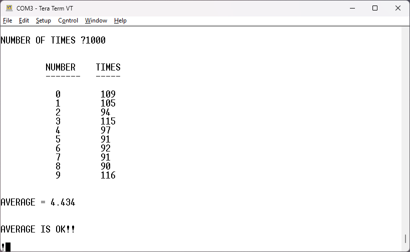
The user manual contains the random.bas
program that "fakes" a floating point number. You can download
this BASIC source code with Tera Term. Because the BASIC
interpreter needs time to store the BASIC lines in memory, the
Tera Term Serial port needs another setup with Transmit delay:
After download you start the BASIC program with RUN. To delete a
BASIC program, you type SCRATCH. Doing 1000 random numbers and the
statistics takes some time.
Grant Searle did a great job in adapting Tandy Color Computer
Microsoft Extended BASIC to his 6809
computer. Tom LeMense adapted the assembler source code to
LWTOOLS assembler and his 6309 computer.
I ported the MSBASIC version to my 6309 computer. The MSBASIC uses
$5C00 to $7FFF in RAM, that is 9216 Bytes. Download the Mon file msbasic.mon (CTRL-A, CTRL-C in the
editor, ALT-V in Tera Term). The source code for LWTOOLS
is in msbasic.asm. The WARM start
address is $5C00, the COLD start address is $5C03.
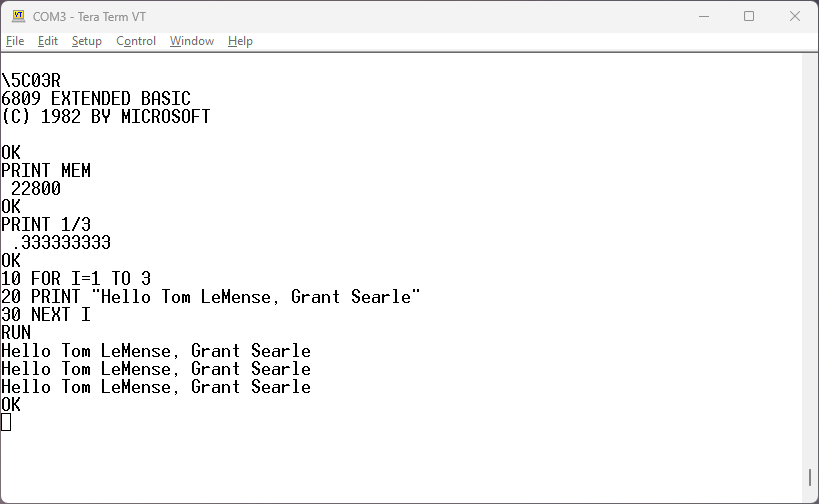
This is Microsoft 9-digit BASIC with 40-bit floating point
numbers.
The definite documentation to Color Computer is COLOR COMPUTER ARCHIVE.
The Unravelled
books discuss the assembler source code. A beginner book for
BASIC is "An Introduction to BASIC programming using the Dragon
micro computer" in the Dragon
32 section.
For me, ChatGPT is a chatbot. The
oldest chatbot of all is ELIZA - A
Computer Program For the Study of Natural Language Communication
Between Man and Machine, a 1966 program by Joseph
Weizenbaum. ELIZA was in 1979 the most interesting program on the
school Commodore PET computer for me. The file eliza.bas is ELIZA for the MSBASIC of my
6309 computer.
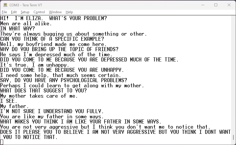
The capitel letter sentences are from ELIZA.
To download eliza.bas into the BASIC interpreter I use two
tricks: First, every BASIC line has eight leading DLE characters
to give the 6309 computer additional time to store the BASIC line
in memory. Second, I add Transmit Delay to Tera Term:

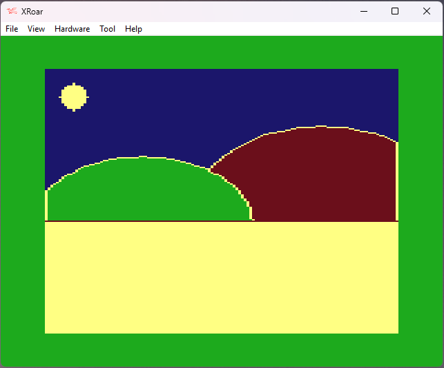
The COLOR
COMPUTER ARCHIVE has the book Creating Adventure Games on
your Dragon 32 by Clive Gifford. I typed "THE DARK FOREST"
adventure and played it on the XRoar Dragon 32
emulator. Like most computer kids in the early 1980s, I started by
typing listings from magazines and books. Can still do it. The
Dragon BASIC has commands for graphics and sound. One example is
the following picture:
You load forest.bas with menu option
"File|Run...". Loading takes some time.
Instructions: You move around the forest by entering the compass
heading, N, S, E or W. Occasionally, you will be asked questions;
usually these are answered with a 'Y' or a 'N'. By typing 'R', you
can choose a number of hours for your character to relax and
increase his or her strength.
I added the command 'M' to show the map:
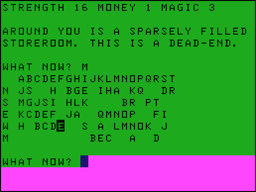 '
'The top row numbers the locations from A to T. Location J is the
prison with no exit. The following four rows N, S, E, W tell the
next location you enter if you go to direction N, ... The row M
tells the random locations of the monsters. You, the player, are
in the "highlighted" location F, the dead-end storeroom with only
exit in direction W.
to be continued ...