Andre Adrian, DL1ADR, 2026-03-22
In the 1970s, lots of companies build 8-bit microprocessors, the Signetics 2650 is one of them. There are rumors that the 2650 was developed in 1972 and had a military life before its civilian life. The 1990 Signetics "Military Products Handbook" says: "Signetics, since 1961, has been dedicated to manufacturing integrated circuits to the stringent requirements of the Defense and Aerospace Industries". Paul Holmes wrote the book "TV Games computer" and said in an interview about the 2650 in USA: "They're low-level classified: the total production is supplied to the military." The 2650 design was done by J. Kessler. The 2650 Restoration Project tells: "At the time of its design in 1972 is was a powerful and elegant microprocessor. However, after it was introduced into the market in 1975 it was quickly overshadowed by other microprocessors." Most important is the comment of "J. Kessler" to Signetics 2650: An IBM on a Chip: "Thanks for the info on the Bally machines. It is interesting my CPU found use after 1972". The 1972 Signetics MOS Data book offers the 2602 NMOS 1024 bits static RAM to the public, the similiar Intel 2102 is from 1972, too. Maybe Intel was second source? There is a hint: The Signetics 2602 has no tri-state Dout pin, the Intel 2102A has.
There are some 1960s minicomputer vibes in the 2650: a build-in hardware stack with 8 entries, an "indirect addressing" bit in the opcode, a program status bit that selects add/sub with carry or without and rol/ror with 9-bit or 8-bit. The 2650 has no "jump on carry/no carry" opcode, only an opcode to translate from carry flag in program status to condition code.
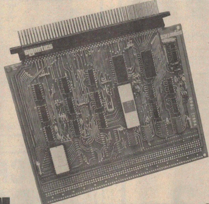
The Signetics 2650 was not as successful as MOS Technology 6502 or Zilog Z80 but is more interesting for me then National Semiconductor INS8060 (SC/MP II), RCA CDP1802 or Fairchild F8 (Mostek 3850). Signetics sold a development board called ABC1500 (Adaptable Board Computer). The kit version was KT9500. IO (Input Output) was seriell RS232 or TTY 20mA loop:
ABC1500 board from advertisment in ETI october 1977 magazine. See 1978 Philips Memories&Microprocessors for details. The white ceramic IC left is the PIPBUG ROM.
The 2650 CPU and 2636 "programmable video interface" are used in
the Radofin "1292
Advanced Programmable Video System". For a short time I had
an "Interton
VC 4000" system, a german 2650/2636 video game console. The
most successful video game console of this time was Atari 2600 or
"Video Computer System". Since 1982 the Emerson
Arcadia 2001 with 2650 CPU and 2637 "universal video
interface" tried to interest customers. Again lots of companies
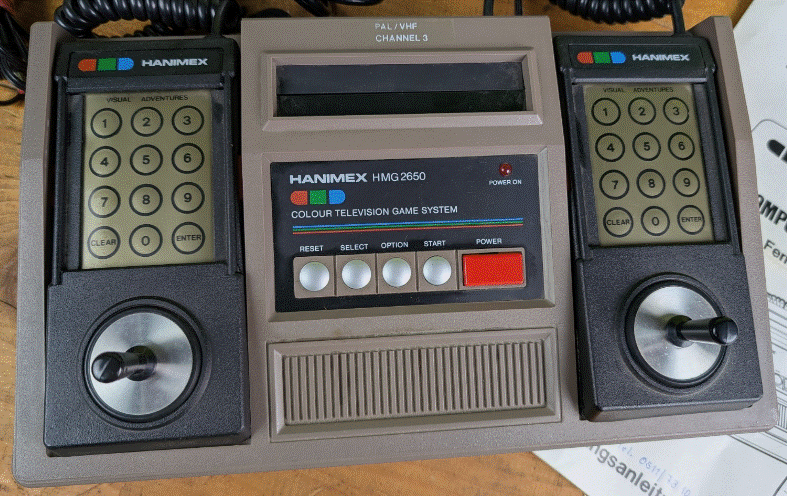
produced similiar systems, like my Hanimex
HMG 2650:
 |
 |
 |
The Signetics 2650 datasheet has an (in)famous "Seven package
minimal system". There is a problem with this schematic.
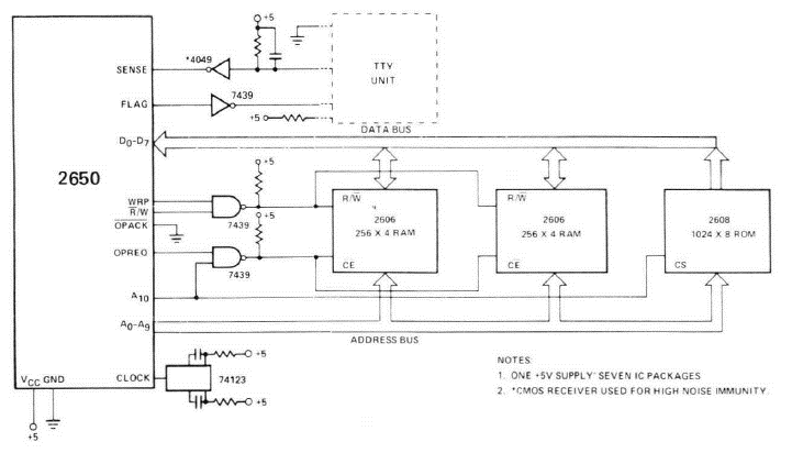
The Signetics 2606 is a 256x4 Bits SRAM (static random access
memory), like Intel 2112 or AMD 9112. The 9112
datasheet tells the sad story about memory devices that have
only /CE and /WE, like the Signetics 2606: "If the external system
[CPU] tries to drive the bus with data, there may be contention
for control of the data lines and large current surges can
result. Since the condition [CPU outputs data, RAM outputs
data] can occur at the beginning of a write cycle, it is important
that incoming data to be written not be entered until the output
buffers have been turned off". Luca
"Tholin" H wrote about his implementation of the Signetics
schematics: "Basically what’s happening here is that the write
enable on those RAM ICs is gated by both R̅/W and WRP (write
pulse), and their chip enable is gated by an address and OPREQ.
The problem with this is that, during a write, the 2650 will put
the correct signals on the address and data buses, use R̅/W to
signal a write and assert OPREQ. Then, it briefly pulses WRP. This
means that, until WRP is pulsed, the RAM ICs are addressed,
enabled, but still in read mode, despite the signal on R̅/W,
as it is NANDed with WRP. Very briefly, the RAM ICs start
outputting data onto the bus at the same time as the 2650. A
signal collision occurs until WRP is pulsed."
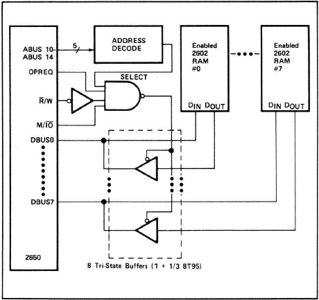
The 2650 has good documentation from Signetics. The application
memo "Address
and data bus interfacing techniques MP53" contains a
schematics about proper use of OPREQ, M/IO and R/W:
A modern SRAM has three different enable pins: chip enable /CE,
output enable /OE and write enable /WE. No data bus action is done
if only /CE is low. Memory read is performed at /CE and /OE low,
memory write at /CE and /WE low. I use all of these signals to
avoid the problem of the Signetics schematics. First my
schematics:
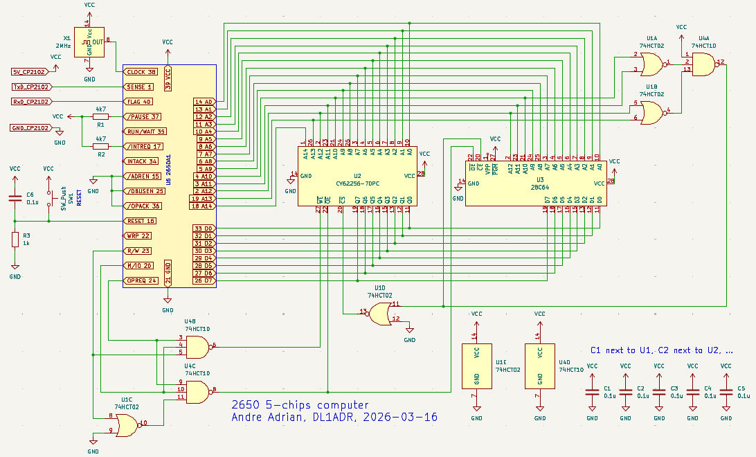
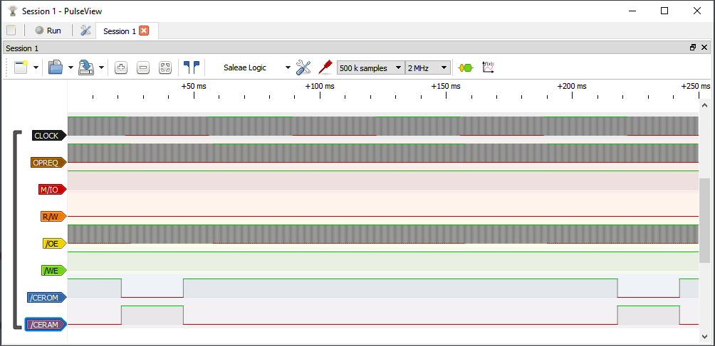
Traditional the /CE is only driven by address bus. The four
address lines A10 to A13 are connected to the /CE logic.The logic
gates U1A, U1B and U4A work together like a 4-input OR gate and
realize the /CEROM. The inverted signal is used as /CERAM. The
EEPROM (electric erasable programmable read only memory) U3 has
/CE active if A10 to A13 are low, that is the address range 0x0000
to 0x03FF and as duplicate 0x4000 to 0x43FF. The RAM U2 has /CE
active if ROM is not selected, that is address range 0x0400 to
0x3FFF and 0x4400 to 0x7FFF. This address layout is compatible to
1 KByte PIPBUG and TCT Basic. For 2 KByte PIPBUG2 the address
lines A11 to A14 are used for /CE. Note: The dual 5-input NOR gate
74LS260 is the better choice for PIPBUG, but hard to get.
The 2650 uses three control bus signals that will be converted
to /OE and /WE. A high level at OPREQ output informs external
devices like ROM, RAM, IO (input output) that action is coming.
The type of action is memory access (M/IO is high) or IO access
(M/IO is low). The two NAND gates U4B and U4C get OPREQ and M/IO
as input signals. For /WE output, the third signal at U4B is R/W.
For /OE output the third input signal to U4C is the R/W output
inverted with U1C. The R/W output is low(!) for read and high(!)
for write - opposite to the 6502 definition of R/W pin. The
problematic WRP is not used.
The HCT logic gates have TTL compatible inputs. LS and HC logic gates should work fine, too.
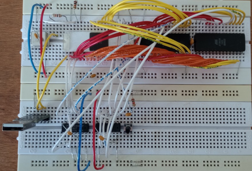
This is the 5-chips 2650 computer on breadboards. Top breadboard
from left to right has quartz oscillator, CPU, RAM and ROM. Bottom
breadboard has USB-to-UART converter (CP2102, CH340), 74HC4002,
74HC10, reset push button. Note: In the final schematic I replaced
74HC4002 with 74HCT02.
The EEPROM has pipbug9600.bin as
program. This is PIPBUG
patched for 9600 baud on a 1.8432 MHz 2650 CPU. More on this topic
below.
I got a 2650A-1 CPU with production date 7838 (year 1978, week
38) as NOS (new old stock). First of all I build a "NOP tester"
and made some measurements. A NOP tester wires the NOP (NO
Operation) opcode $C0 to the data bus and wires the control bus
input signal appropriate. For the 2650 these are:
RESET (16) 1 kOhm to GND, 0.1uF to VCC.
CLOCK (38) TTL level clock, I used 250 kHz.
/OPACK (36), /ADREN (15), /DBUSEN (25) to GND.
/INTREQ (17) 10 kOhm to VCC.
/PAUSE (37) 10 kOhm to VCC.
SENSE (1) 10 kOhm to VCC.
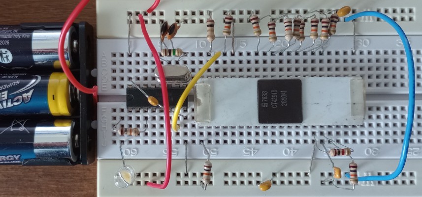
The IC left is a 74HC4060 with 4 MHz quartz, I still have to order
a proper clock source. 8 resistors 10 kOhm are used to set the
opcode.
I have a little Logic Analyzer (LA) with 8 channels and USB
connection to the computer. Unfortunately, the OS-driver for the
USB device is not working with MS-Windows 11, but it works with
MS-Windows 10.
The first LA screen shot shows the NOP tester with opcode $C0, NOP:
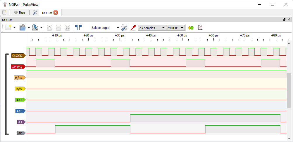
The NOP opcode does nothing, next to fetch an 1-byte opcode. NOP
has a timing of 2 cycles. Every cycle has 3 clocks. We see that
the OPREQ=high has a timing of 1.5 clocks.
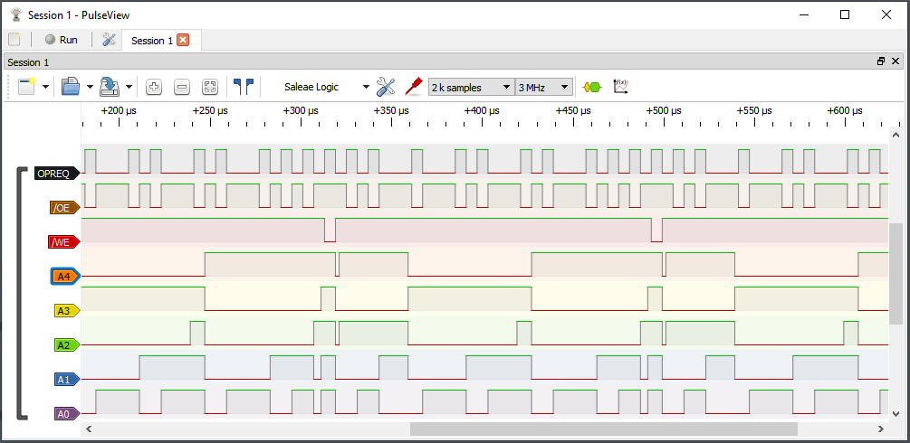
The second LA screen shot shows the NOP tester with opcode $70, REDD,R0:
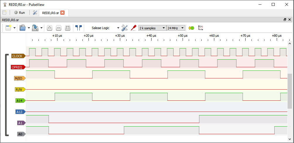
The REDD,R0 opcode first fetches the 1-byte opcode, then fetches
an 1-byte IO byte. Only the address lines A14 and A13 are
important for this IO operation. A13 or E/NE tells the IO devices
"this is non-extended IO" and A14 or D/C tell "this is data IO".
Note: next to data IO there is control IO. Next to non-extended IO
there is extended IO with one byte address range.
The 2650 NOP is a "slow" opcode having only one memory access in
two cycles. The REDD (read data) is a "fast" opcode with one
memory access and one IO access in two cycles.
After I wired clock oscillator, CPU and the two glue logic chips
74HCT02, 74HCT10, I measured the extended NOP tester:
The CPU marches, driven by NOP opcode, from address 0x0000 to
0x1FFF, that is the lower 8 KByte. In a small part of this memory
range, /CEROM is active (low), in a larger part /CERAM. Now I can
attach ROM and RAM and try out the first program.
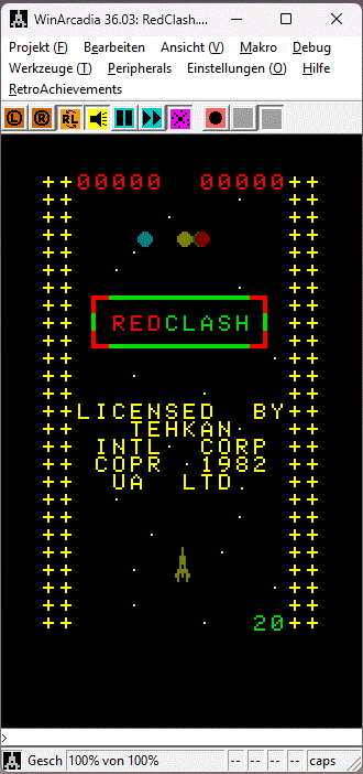
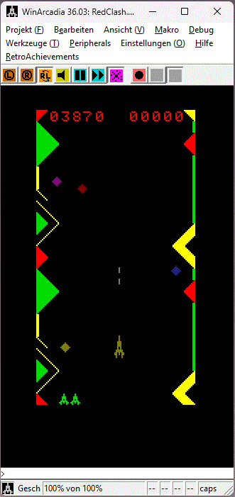
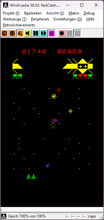
WinArcadia for MS-Windows
computer is a simulator for 2650 computers like the Interton VC
4000 (2650/2636 video game console) and the PIPBUG home computers.
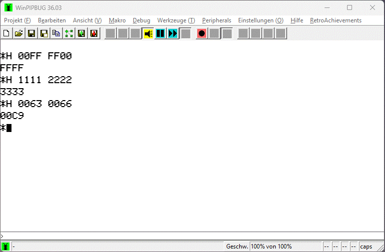
Screen shot: WinArcadia as PIPBUG2 home computer simulator. The
PIPBUG2 command H performs hexadecimal 16-Bit addition.
WinArcadia is a development environment, too. You can assemble
programs, you can write Bin files for the EEPROM programmer. First
program has two purposes: First verify the /WE part of the
hardware, second input from the SENSE pin and output to the FLAG
pin. I connect a push button between SENSE pin and GND. A 10 kOhm
resistor is already in place. And I connect a low current white
LED with a series 10 kOhm resistor between FLAG pin and VCC (+5V).
Next topic is the program:
; COLD start for a 2650/2636 machine
COLD:
BCTA,UN
RESET ; goto RESET:
INTERRUPT:
RETC,UN ; return
from interrupt
RESET:
LODI,R0
$20 ; R0 = 0x20
LPSU
; PSU = R0
LPSL
; PSL = R0
; the program
forever:
; for (;;) {
SPSU
; R0 = PSU
BCTR,N
else3 ; if (0 == SENSE) {
CPSU FLAG
; FLAG = 0
BCTR,UN endif3
else3:
; } else {
PPSU FLAG
; FLAG = 1
endif3:
; }
STRA,R0
$1FFF ; *0x1FFF = R0
BCTR,UN forever ; }
The complete program is first.asm. The Bin file is first.bin and contains 22 bytes. The first lines are defensive programming for a 2650 computer with interrupts. The opcode SPSU reads all bits of program status upper (PSU) into accumulator R0. The SENSE bit is bit 7. If bit 7 is set, the condition code reports "Negative". The opcodes CPSU resets (CLEAR) only the FLAG bit and PPSU sets (PRESET) the FLAG bit.
The 2650 CPU has on-chip a 1-bit input pin SENSE and a 1-bit
output pin FLAG. The Signetics application memo "SS50
PIPBUG" uses bit-banging, the colloquial term for doing
serial IO by software. The following "PIP assembler" program chin9600.asm changes PIPBUG to 9600 baud
at 1.8432 MHz clock speed. Select PIPBUG machine in WinArcadia,
assemble the patch program and savebin 0 3FF for PIPBUG in Bin
file.
ORG $286
CHIN:
; 9600 baud input 1.8432 MHz
clock
PPSL RS
; Alternate regs
LODI,R0
$80
; Enable tape reader
WRTC,R0
LODI,R4 0
LODI,R5 8
ACHI:
SPSU
; 2
BCTR,LT
ACHI ; 3 Look for
start bit
EORZ R0 ;
2
WRTC,R0 ;
2 Disable tape reader
BSTR,UN
DLY ; 3
; 1.8432 MHz 9600 baud 0.5
bit time = 32 cy
; 3*3+4*2-2.5=14.5 N=6
BCHI: BSTR,UN DLAY ;
3 Wait to middle of data
SPSU
; 2
ANDI,R0
$80 ; 2
RRR,R4
; 2
IORZ R4 ;
2
STRZ R4 ;
2
BDRR,R5
BCHI ; 3
; 1.8432 MHz 9600 baud 1 bit
time = 64 cy
; 4*3+6*2=24 N=13
BSTR,UN DLAY
ANDI,R4
$7F
; Delete parity bit
LODZ R4
CPSL RS+WC
; Standard regs, 8-bit
rotate
RETC,UN
; return char in R0
ORG $2A8
DLAY:
; DELAY FOR ONE BIT TIME
LODI,R0
13 ; 2
BCTR,UN
DLY2 ; 3
NOP
ORG $2AD
DLY:
; DELAY FOR 0.5 BIT TIME
LODI,R0
6 ; 2
DLY2 BDRR,R0
$ ; 3
RETC,UN ;
3
NOP
NOP
ORG $2B4
COUT:
; output
PPSL RS
; Alternate registers
PPSU FLAG
; Stop bit level
STRZ R5
LODI,R4 8
BSTR,UN DLAY
BSTR,UN DLAY
CPSU FLAG
; Start bit level
ACOU: BSTR,UN DLAY ; 3
RRR,R5
; 2
BCTR,LT
ONE ; 3
CPSU FLAG ;
3 Data bit = 0
BCTR,UN
ZERO ; 3
ONE: PPSU
FLAG ; 3 Data bit = 1
ZERO: BDRR,R4 ACOU ; 3
; 1.8432 MHz 9600 baud 1 bit
time = 64 cy
; 7*3+2*2-1.5=23.5 N=13
BSTR,UN DLAY
PPSU F
; Stop bit level
CPSL RS
; Standard registers
RETC,UN
The subroutine entry point is at label CHIN. The subroutine "busy
waits" at label ACHI until the SENSE CPU pin detects low level.
Note: The USB-to-UART converter has inverted output /TxD. Next a
half bit time delay is waited. Now the data bits are received with
wait a bit time, read the level of SENSE bit and shift the
received bit into R4. After 8 bits are received, the topmost bit
is cleared (Delete parity bit) and the subroutine returns.
To make bit-banging work, the timing of the CPU has to match the
timing of the IO. First you write the opcode duration in cycles
(cy), then you calculate the average duration without the time
spend in a BDRR,R0 loop and last you calculate the proper BDRR
loop counter (init) value. Note: I disassembled the subroutines
CHIN, DLAY, DLY from the PIPBUG in the WinArcadia simulator. There
are little changes to the 110 baud at 1MHz CPU clock of the
original PIPBUG listing.
As USB-to-UART converter I use a ready made little PCB with
CP2102 chip. Please download the MS-Windows CP2102 driver from www.silabs.com.
I had problems with outdated driver on MS-Windows 11.
I use Tera Term terminal emulation on the "host computer", an
MS-Windows 11 PC. As always, Setup Serial port and Setup Terminal
are important:
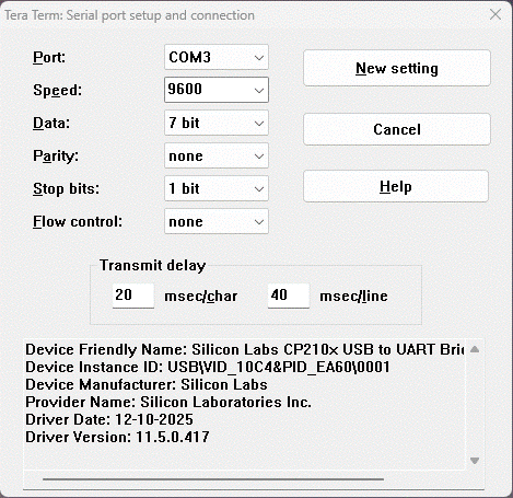
The Terminal emulator uses 9600 baud, 7n1 (7 data bits, no
parity, 1 stop bits). Because we have no flow control, we need
transmit delay to match the slow 2650 computer to the fast host
computer. Note: The MS-Windows 11 real time behavior is bad.
Measured time between one character and the next ranges from 20 ms
to over 30 ms. Too small values for transmit delay create USB
communication loss and re-establishment.
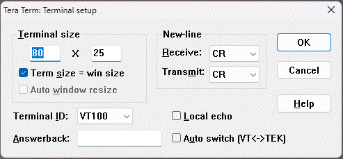
The Terminal setup is nothing special. But PIPBUG has special
needs. Some PIPBUG commands use CR to do the one thing and LF to
do the other thing. This terminal setup puts CR on the RETURN key
and LF on the CTRL-J key. For "EOL (end of line) Conversion" in
Notepad++ editor, the 2650 computer is a Macintosh.
The PIPBUG uses the command D to "upload" a program to the host
computer and command L to "download" a program from the host
computer. In 1976, upload was called DUMP and download was called
LOAD. The format of dump and load was called "papertape", because
normally the "storage medium" was the 9-holes paper
tape of the ASR-33 110 baud ASCII teletype. The papertape
format is:
1 character :
4 characters hex address
2 characters hex record length (0 to 255)
2 characters hex header checksum
2*N characters hex data
2 characters hex data checksum
1 character CR
The "EOF" papertape block is:
:044000
This is a header with program_entry_address=0440 and len=00.
At Dump, a longer program is split in 255 bytes "chunks". The Load reads chunk after chunk until an EOF block is read.
At download there is no indication of download complete. A LED
with series resistor to VCC (+5V) at the /TxD line helps. My
CP2102 USB-to-UART board has LEDs on board.
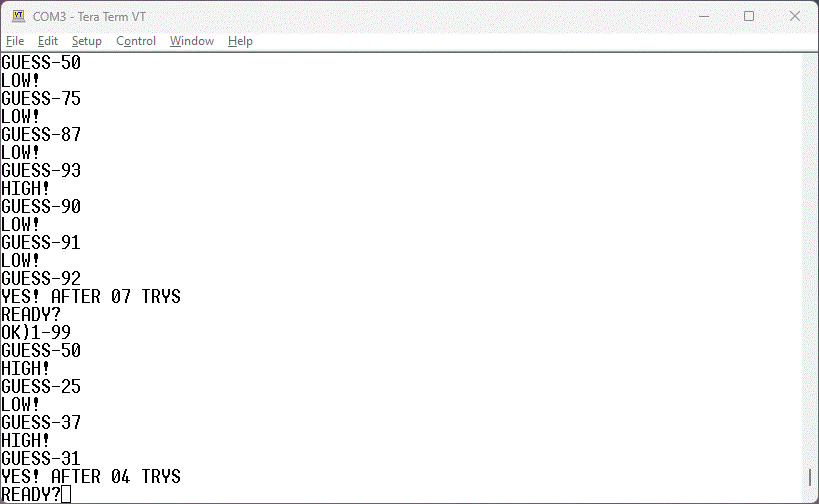
My first "computing device" was a programmable pocket calculator.
And the most interesting program was "Guess the number" game. This
fun of the 1970s you can have with the 2650 computer, too.
WinArcadia has programs in AOF format, that is PIPBUG papertape
format. You only have to set "EOL conversion" in Notepad++ editor
to "Macintosh (CR)" for PIPBUG on a REAL computer. I even added L
to the AOF file to make it "plug and play". Last but not least,
the EOF block has to have 8 hex characters. Open file GuessingGame-MachineCode.aof
in Notepad++, select all CTRL-A, copy CTRL-C and paste to Tera
Term with ALT-V. I repeat: ALT-V, not CTRL-V. Then
you can play this famous game:
 |
 |
The registers are the fastest memory in the computer system. The
2650 has 7 registers with 8-bit. The registers R1, R2, R3 have an
alternate register set R4, R5, R6. The opcode CPSL RS
selects the normal registers, opcode PPSL RS selects the
alternate registers. In my opinion this is easier to understand
than the Z80 toggle opcode EXX. Note: RS is an EQU
for $10.
The registers R1 to R3 are like the universal registers D0 to
D7 in the 68000 for register-memory opcodes. The C language
statement add constant R1 += 3 translates directly into ADDI,R1
3. The add memory statement R3 += addend translates to ADDA,R2
addend for absolute address or ADDR,R2 addend for
PC-relative address.
For register-register opcodes, R0 is the accumulator. The
statement R0 += R3 translates to ADDZ R3, the statement
R3 += R0 is not possible.
Unsigned 8-bit multiplication with 16-bit result is easily done
with registers R0 to R3. The multiplier goes into R1, the
multiplicand into R2. The result upper 8-bit goes to R0, the lower
8-bit goes to R1, the multiplier gets overwritten in the "fast
multiplication" algorithm. We need one register for the "bit
counter" and use R3.
UMUL8:
; R1=multiplier, R2=multiplicant
EORZ R0 ;
result_high = 0
LODI,R3
9 ; bit_counter = 9
CPSL C ;
carry=0
BCTR,UN strt2
do2:
; do {
TPSL C
; if (carry) {
BCTR,LT endif2
CPSL C
; prdh += mltd
ADDZ R2
endif2:
; }
RRR,R0
; prdh >>= 1
strt2:
RRR,R1
; mltr >>= 1
BDRR,R3
do2 ; } while (--cnt > 0)
RETC,UN ; result
in R0 (high), R1 (low)
The ready to assemble file for e.g. Interton VC 4000 is umul8.asm. The comments are pseudo C
language. The carry flag working is not correctly expressed in
these comments. The 2650 assembler program is not (completely)
structured, either. Instead of explaining the program step by
step, I suggest to execute the program step by step in WinArcadia.
See Getting
Started for WinArcadia instructions.
Before we do 16-bit arithmetic, we ask: is 2650 a big-endian or a
little-endian CPU? Because there are no 16-bit arithmetic opcode,
we can decide ourselves. But, the absolute addresses in opcodes
are big-endian and the assembler ACON pseudo-opcode defines a
16-bit big-endian constant, I declare 2650 big-endian (for
now).
For extension to 16-bit multiplication with 32-bit result we have
to consider that rotate opcodes are only possible for register and
prdh and mltr need rotate. Second, only R0 can do
register-register addition. Therefore we put prdh into R0, prdh+1
into R1, mltd in R2 and leave mltd+1 in memory, mltr into R4,
mltr+1 into R5 and bit_counter into R3.
UMUL16:
; R4,R5=multiplier, R2,mltd+1=multiplicant
EORZ R0 ;
result_high = 0
STRZ R1
LODI,R3
17 ; bit_counter = 17
CPSL C ;
carry=0
BCTR,UN strt2
do2:
; do {
TPSL C
; if (carry) {
BCTR,LT endif2
CPSL C
; prdh += mltd
ADDR,R1 mltd+1
ADDZ R2
endif2:
; }
RRR,R0
; prdh >>= 1
RRR,R1
strt2:
PPSL RS
RRR,R4
; mltr >>= 1
RRR,R5
CPSL RS
BDRR,R3
do2 ; } while (--cnt > 0)
RETC,UN ; result
in R0 (high), R1, R4, R5 (low)
The ready to assemble file is umul16.asm.
I hope, the similarities and differences between UMUL8 and UMUL16
are easy to see and understand. Now multiplier uses R4 and R5 with
R4 the higher byte and R5 the lower byte. The pseudo C comment
uses now 16-bit data types. The comments shall have a higher
abstraction level then the assembler listing. With Z80 I
have done 64bit = 32bit * 32bit multiplication with registers in
the 1980s.
The 16-bit division uses rotate left and subtraction as the main
ingredients, opposite to multiplication that uses rotate right and
addition. If the subtraction fails, an addition does undo it. The
traditional division for 6502 stores the values before subtraction
for undo.
UDIV16:
; R4,R5=dividend R2,dsor+1=divisor
EORZ R0 ; rema =
0
STRZ R1
LODI,R3
16 ; cnt = 16
do3:
; do {
PPSL RS
; dend <<= 1
CPSL C
RRL,R5
RRL,R4
CPSL RS
RRL,R1
; rema <<= 1
RRL,R0
PPSL C
; rema -= dsor
SUBR,R1 dsor+1
SUBZ R2
TPSL C
; if (!carry) {
BCTR,LT else3
PPSL RS
; dend |= 1
IORI,R5 1
CPSL RS
BCTR,UN endif3
else3:
; } else {
CPSL C
; rema += dsor
ADDR,R1 dsor+1
ADDZ R2
endif3:
; }
BDRR,R3
do3 ; } while (cnt > 0)
RETC,UN ;
R4,R5=quotient R0,R1=remainder
See udiv16.asm for assemble file. If
subtraction with carry is used, the carry flag has to be set, like
for the 6502. Division has the special case of "divide by 0" which
normally forces program abort. This is not implemented, but easy
to do.
For 16-bit signed division, first dividend and divisor have to be
changed to positive values, then do unsigned division and last
apply the quotient sign as exclusive-or of dividend and divisor
signs.
My opinion about 2650 "number crunching": Registers are good for
you (like Guiness beer). That there is no "branch if no carry"
opcode, instead you need CPSL C and BCTR,LT endif2
is "1960s minicomputer vibes". The registers R1 to R6 have more
8-bit computing power then B to L' registers of Z80, but no 16-bit
computing power. A pity that there is no CMOS version of the 2650
with higher clock speeds like 4 MHz. There are some quirks with
2650 assembler, but of all assembler I know (Zilog Z80, Motorola
68000, Intel 8086, MOS Technology 6502) the 2650 is most straight
forward.
The Z80 assembler udiv16.z80 is shorter
then the 2650 version. The 16-bit accumulator HL and the 8-bit
accumulator A help:
UDIV16:
; C,A=dividend D,E=divisor
ld
hl,0 ; rema = 0
ld
b,16 ; cnt = 16
do3:
; do {
add
a,a
; dend <<= 1
rl c
adc
hl,hl ; rema
<<= 1
or
a
; rema -= dsor
sbc hl,de
jr
c,else3 ; if (!carry)
{
inc
a
; ++dend
jr endif3
else3:
; } else {
add
hl,de
; rema += dsor
endif3:
; }
djnz
do3 ; } while (cnt
> 0)
ret
; C,A=quotient H,L=remainder
The 6502 assembler udiv16.65s needs 6
bytes in the zero page.The 2650 and Z80 use the same algorithm,
the 6502 is slightly different:
dend = $00 ;
2 dividend, quotient
dsor = $02 ;
2 divisor
rema = $04 ;
2 remainder
udiv16:
; dend=dividend dsor=divisor
LDA
#0 ; rema
= 0
STA rema
STA rema+1
LDX
#16 ; cnt = 16
do3:
; do {
ASL
dend ;
dend <<= 1
ROL dend+1
ROL
rema ;
rema <<= 1
ROL rema+1
LDA rema
SEC
; AY = rema - dsor
SBC dsor
TAY
LDA rema+1
SBC dsor+1
BCC
endif3 ; if (carry) {
STA
rema+1 ;
rema = AY
STY rema
INC
dend
; ++dend
endif3:
; }
DEX
; while (--cnt)
BNE do3
RTS
; dend=quotient rema=remainder
Code density of Z80 is best (22 bytes), of 2650 (39 bytes) is
worst and 6502 (38 bytes) is nearly as 2650.
The PIPBUG 1 KByte monitor was part of the 1976 PC1001 board from
Signetics. See Signetics
SS50 PIPBUG applications memo.
The PIPBUG2 2 KByte monitor was part of the 1979 CP1002 mask of
the 2556 SMI (System Memory Interface). This was an integrated
circuit with 2 KByte ROM, 128 Byte RAM and 8 bit IO. See Philips
TN132 The 2656 CP1002 system memory interface Technical
Note.
The PIPBUG2 ROM contains PIPLA, a little 2650 assembler.
To be continued ...
MicroWorld BASIC is an 8 KByte BASIC for 2650, Copyright
MicroWorld, 1979. On the Binnie Home Page is the MicroWorld
BASIC manual. The "ready-to-download" program file for
PIPBUG is MicroWorldBASIC.aof.
Open the AOF File in Notepad++, select all CTRL-A, copy CTRL-C and
paste to Tera Term with ALT-V. Download takes some time.
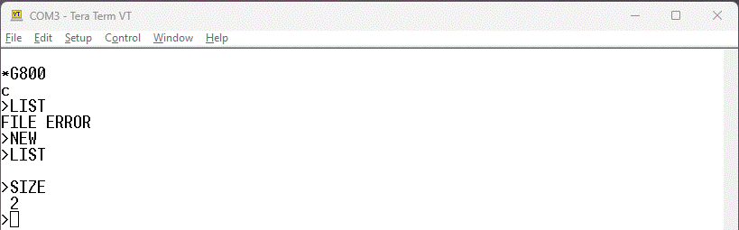
One important detail is somehow hidden in section "YOUR FIRST
PROGRAM" on manual page 11: "After typing NEW (or just N), type a
Carriage Return". The MircoWorld BASIC command SIZE tells the size
of the BASIC program in memory and optional the size of the BASIC
variables.
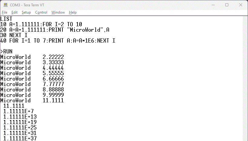
The program fptest.bas shows the
floating point quality of MicroWorld BASIC. I assume mantissa is
BCD and exponent is binary, the exponent range of -64 to +62 let
me assume this. MicroWorld BASIC uses CR only as line terminator,
like Apple Macintosh.
The PHUNSY section of WinArcadia games has OTHELLO.bas,
an Othello game in dutch. PHUNSY
is a 2650 computer by Frank Philipse, well known for tube data
sheets.
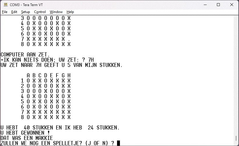
The computer plays very slow, but it should be easy to translate
the 199 lines of BASIC source code into assembler. As far as I
see, the program don't need floating point numbers.
The BASIC program needs a lot of time to store the downloaded
BASIC line into BASIC memory. The Tera Term program and/or the
USB-to-UART driver have a problem with large "Transmit delay"
duration. Therefore I use the old "waiting with DLE characters"
trick. You add "don't care" characters after CR to give the BASIC
program time to do the storage work. I use 0xFF instead of DLE
(0x7F) because Tom Pittman wrote in TINY BASIC User Manual: "The
pad character ... is set by default to the "Rubout" or Delete code
(hex FF ...) to minimize synchronization loss for bit-banger I/O
routines". The 2650 computer uses bit-banging. Every 0xFF or DLE
character received, the MicroWorld BASIC acknowledges with a >***
output. There are 12 pad characters per line, but sometimes you
see only one of the >*** outputs. Then the duration
of 11 characters or 220 ms (because of transmit delay) were used
to store the BASIC line. The binary search in the TinyBasic
patch helped a lot to reduce this duration.
The WinArcadia simulator contains TCT Basic. The authors are T.
Long, C. Barratt and T. Wooller and the year was 1978. TCT Basic
needs 4 KByte and works together with 1 KByte PIPBUG monitor.
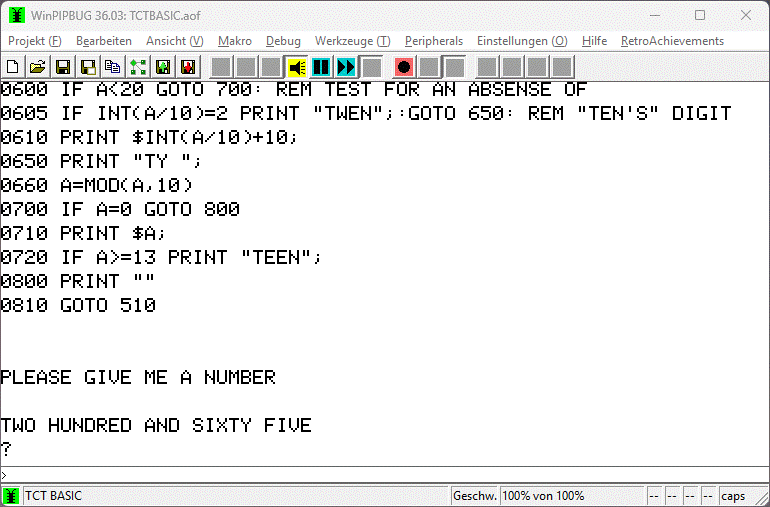
The 2650
Restoration Project has more information about TCT Basic.
You can load the tct_demo.bas source
code into TCT Basic with the WinArcadia "Insert text" menu
command. Note: 110 baud is REALLY slow. You can set WinArcadia to
300 baud.
To be continued ...